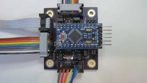
Photo 1. Assembled MIO Board
The following describes a custom PC board, as shown in Photo 1, that is designed to host an Arduino Pro Mini processor and provide a convenient way to connect its I/O to external circuits. In the following, the Mini I/O board is called the MIO board. The board is available from the author (see email address below the Revision History section.
The MIO board is designed to provide a compact and convenient way to access the Pro Mini I/O ports. Connections are brought out on three shrouded 2x5 IDC plugs with each plug breaking out 5 I/O pins and providing ground and power connections on the remaining 5 pins.
Use of shrouded connectors ensures that cables connected to the MIO board are properly keyed. Typically, connections are made with ribbon cable with 2x5 IDC sockets at the MIO board end. Connections on the other end of the I/O cables can be terminated on another 2x5 connector or wired directly to external circuits and components. For example, a cable could connect directly to an incremental encoder and switch assembly that requires power, ground, two encoder phases and a switch connection.
The following describes the use and features of the MIO board.
Photo 2 shows the top side of an unassembled MIO board. The vertical rule alongside the board shows the approximate scale.
Photo 3 shows the bottom side of an unassembled MIO board. The horizontal rule alongside the board shows the approximate scale.
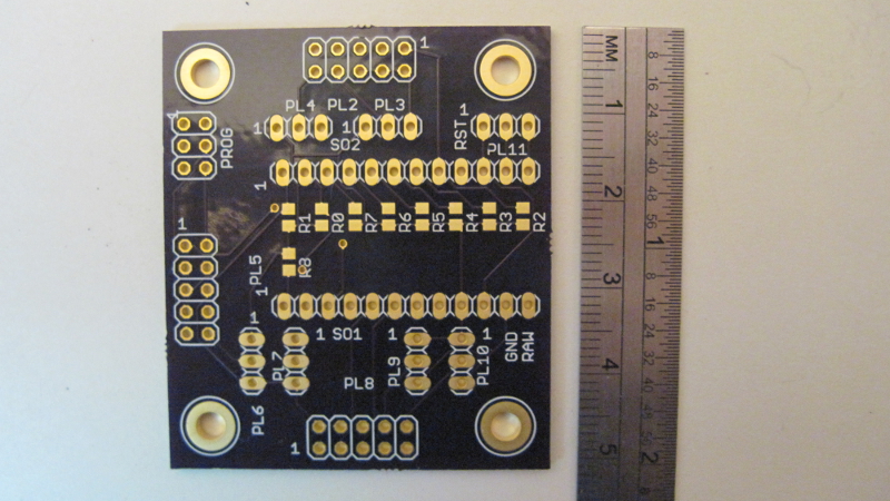
Photo 2. Bare MIO Board, Top Side
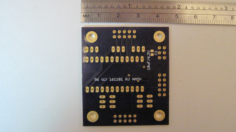
Photo 3. Bare MIO Board, Bottom Side
The size of the board is 2 by 1 3/4 inches (51 by 45 mm). The hole spacing along the 2 inch side is 1 5/8 inches (41 mm) and along the smaller side it is 1 3/8 inches (34 mm). The holes are 1/8 inch (3 mm) in diameter. The mounting holes are gold plated but not connected to ground or other board circuitry.
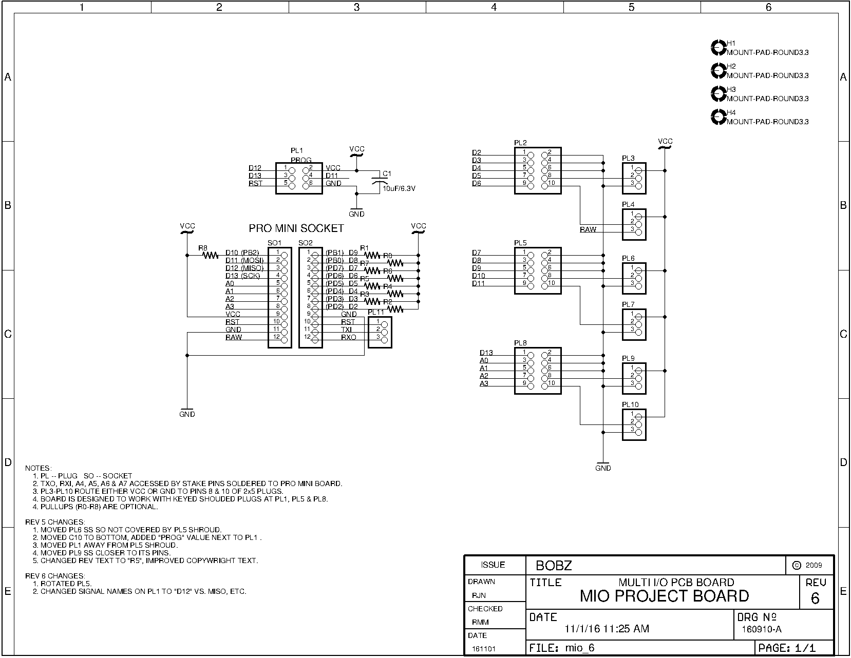
Schematic 1 shows the MIO component connections. Photo 4 shows a top view of the unassembled and assembled board. The following sections describe the board components and their interconnections.
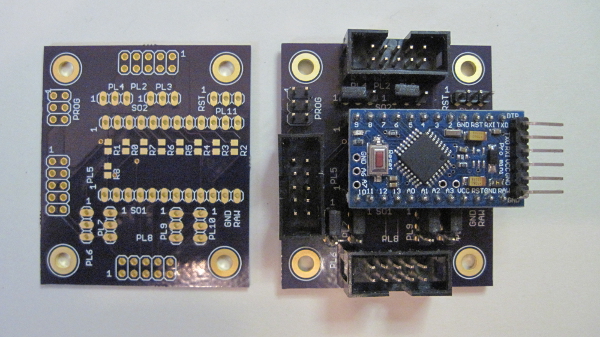
Photo 4. Bare and Assembled MIO Board, Top View
As shown in Photo 4, the Pro Mini board mounts on the middle right side of the board with the Pro Mini external interface pins facing toward the outside of the MIO board. Silk screen annotation for "RAW" and "GND" at the bottom right corner of the Pro Mini footprint should correspond exactly with the same silk screen markings on the Pro Mini board.
The Pro Mini board is normally mounted on MIO board socket pins but can be soldered directly to the MIO board for increased reliability and a lower vertical profile.
Schematic 1 shows the Pro Mini socket connections as "SO1" and "SO2." These designations are also shown on the top side silk screen at approximately pin 4 of each socket.
To mount the Pro Mini on a socket, insert the Pro Mini pins into a 12-pin socket strip and then insert the socket strip pins into the MIO board. This ensures that the socket fits exactly. The socket pin strips can be soldered to the MIO board separately, but the strips must be vertically aligned so that each of the socket strips are vertical with the bottoms flush to the board along the entire socket length. This can be done by tack-soldering one pin of each socket strip and then aligning the socket strip eye (from the edge of the board) as the pin is re-heated. Once the socket strip is wiggled in place and vertically aligned, the remaining pins can be soldered.
To make it easier to insert the Pro Mini correctly, one of the end socket pins can be painted along with the end plug pin of the Pro Mini, so that they are both marked. Pin 1 of SO1 is a good choice for this marking, as it corresponds to the normal DIP position for pin 1. Using this scheme, the Pro Mini is treated as a large DIP IC with the "D10" marking on the Pro Mini corresponding to pin 1 of the DIP.
The reset and serial I/O connections from the Pro Mini are brought out to PL11, located at the top right of the board, as shown in Photo 3 and Photo 4.
The reset connection is useful for applications where a user reset is required without access to the reset switch on the Pro Mini board. Avoid long wire connections to this pin, especially where strong AC or RF fields are present. Connections to this pin may have to be bypassed or isolated with a ferrite bead to avoid "flakey" behavior.
The serial connections on PL11 simply duplicate those on the Pro Mini board. These connections are also available on the 1 by 6 pin header on the end of the Pro Mini board. These connections are convenient monitoring points for the serial link and may also be used to drive an external serial connection (e.g., another Pro Mini board).
Pullup resistors can be added to many I/O pins, as shown in Schematic 1. The pullup resistors are designate R0 through R8 and apply to pins on Port B and Port D (i.e., PB0-2 and PD2-7).
If installed, pullups should be soldered to the MIO board before any other components such as sockets or stake pins. This avoids melting the plastic pin carriers by the heat gun.
A 2 by 6 pin header, PL1, provides a connection for a standard hardware programmer interface such as a USBTiny. The programmer interface pins pins are located in the upper left corner of the board, as shown in Photo 2 and Photo 4. Photo 1 shows a gray cable connected to this interface.
The programmer interface is not keyed so the user must ensure that the programming cable is correctly oriented. Pin 1 is clearly marked on the board to aid in proper cable orientation.
The programmer interface pins, when not connected to a programmer, can be used to access power and ground connections (pins 2 and 6, respectively) and to access the SPI interface pins, MISO (pin 1), MOSI (pin 4) and SCK (pin 3). Reset is also available on PL1 (pin 5).
A bypass capacitor, C1, can be installed near the programmer pins; the 0805 SMD footprint for this capacitor is located on the bottom of the board, as shown in Photo 3. Although this capacitor can be installed any time during the board building process, it is normally installed first or installed along with any pullup resistors.
The bulk of Pro Mini connections are provided by three 2 by 5 headers, PL2, PL5 and PL8 (see Schematic 1). The connections are intended for use with shrouded, keyed connectors, as shown in Photo 4. Photo 1 shows these connectors with cable connections.
The use of keyed connectors prevents mis-connections when cables are connected and reconnected. This is particularly important during the development and maintenance phases of a project where cabling may be connected and disconneted many times.
The use of keyed connectors and color-coded ribbon cable also allows color-coded connections to be extended to attached component assemblies.
Each connector provides connections for five pins of Pro Mini I/O. These connections are provided on the odd-numbered pins (pins 1-9). Even-numbered pins provide ground (pins 2-6) or an option for connection to power or ground (pins 8 and 10).
The connector pin arrangement is designed so that I/O that requires a ground reference or connections that must furnish power to an external component have in-cable access to these connections. For example, a cable connecting to an optical incremental encoder with an associated switch might furnish connections for A and B phases, a switch connection and associated ground references and a power connection. All of these connections can be easily provided in a single keyed, color-coded, detachable cable.
As shown in Schematic 1, PL2 provides I/O connections for Pro Mini pins D2 through D6. PL5 provides I/O connections for Pro Mini pins D7 through D11. PL8 provides I/O connections for Pro Pini pins D13 and A0 through A3.
There is no provision to directly access D12 (MISO) with one of the three I/O connectors. This signal can be accessed at the programming connector, however.
The omission of D12 is arbitrary and based on my current project I/O usage. It is also assumes that any extension of the SPI port will be provided through a cable connection to the programming connector, PL1. Because MISO represents a connection from an external device into the Pro Mini board, connection via PL1 is a useful alternative.
Also, there is no provision for keyed connections to off-grid breakout headers for A4, A5, A6 and A7. These are provided on internal board pads of the Pro Mini board but are diffucult to bring out on socket connections. It is assumed that these connections will be brought out directly from stake pins soldered to the Pro Mini board or to I/O connectors PL2, Pl5 or PL8 via their option headers.
The following section describes how D12 and pins A4 to A7 can be brought out from the keyed connectors using the option jumpers.
Schematic 1 shows how the option jumpers PL3, PL4, PL6, PL7, PL9 and PL10 provide power or ground connections to pins 8 and 10 of the I/O connectors.
For PL2, pins 1 and 2 of PL3 can be jumpered (e.g., with a Berg jumper) to provide MIO board Vcc to pin 8. Jumpering pins 2 and 3 of PL3 connects pin 8 to ground.
Also for PL2, pins 1 and 2 of PL4 can be jumpered to provide Vcc to pin 10. For PL2 only, jumpering pins 2 and 3 of PL4 connects the RAW input pin on the Pro Mini to pin 10. Normally the RAW input is from an external power source and feeds the on-board 5 Volt or 3.3 Volt regulator. The PL4 jumper option allows the raw DC from an external source to be fed into the board via PL2.
If the Pro Mini's on-board regulator is removed (e.g., for low-power operation), the RAW "input" can be used to bring out (or bring in) other I/O to or from the board, as described below for the option jumpers for PL5 and PL8.
The option jumpers for PL5 and PL8 provide power or ground connections for pins 8 and 10 for the respective plugs, as described above for PL2.
The option jumpers for PL2, PL5 and PL8 can also be used to bring out selected I/O from the MIO board via pin 2 of the PL3, PL4, PL6, PL7, PL9 and PL10 option jumpers. For example, a wire-wrap jumper from pin 1 of PL1 to pin 2 of PL3 brings out the D12 (MISO) connection to PL2.
Similarly, the pin 2 connections on the other option jumpers can be used to bring out the "analog" pins via wire-wrap jumpers to pins or to solder pads on the Pro Mini board.
Although connecting I/O through the keyed connectors with color-coded ribbon cable is a convenient way to connect to project parts and assemblies, there are other useful connection alternatives.
One alternative that is particularly useful during development is to connect to the I/O connector pins with socket wires that can be connected to a solderless breadboard or to instrumentation. This connection alternative is shown at the bottom of Photo 1. This alternative retains the ability to color-code the wiring.
Another convenient alternative is to break out the I/O wiring to a screw-down connector. One way to do this is to use a 10-pin cable between the MIO board and an IDC to screw-down connector board.
Of course, direct-wired connections via the MIO board's solder pads provides the greatest reliability, especially for projects operating in harsh environments (e.g., high vibration, humidity) where IDC connectors cannot provide reliable connections. We have found that "CPC" (military) type connectors provide high reliability because of their round pins, high contact surface and ability to be made water-tight with a gasket and cable seal.
Added sections for option jumpers and connection alternatives. |
||
Added info on option jumpers |
||
Initial release |
Copyright © 2016, Bob Nash.