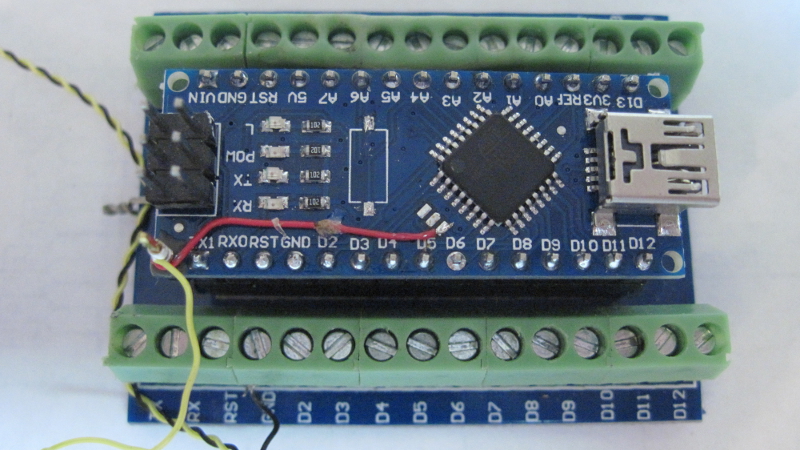
Photo 1. DECA Decade Counter Board
This manual describes the construction and operation of the DECA decade counter board. The board consists of a a standard NANO board with custom hardware and software modifications needed to make a decade counter for a 10 MHz input signal.
The board, with a custom hardware modification (jumper wire), is shown in Photo 1 above.
The following describes the software programming and hardware modifications needed to produce the board. Also described are the capabilities of the board, including a link to a schematic showing the available decade divider outputs.
Although the DECA board can be used standalone to provide divided outputs from a source such as a "can-type" crystal oscillator, it is primarily intended for use with a precision source such as a rubidium reference oscillator. Also, the DECA board is a key module in the BOBZ DECA-FEBO board for use with a rubidium reference. The DECA-FEBO board provides a plug-in interface to a rubidium reference that provides divided and multiplied outputs derived from the reference oscillator.
The DECA decade counter board consists of a NANO board modified to accept an external clock and loaded with a carefully-tuned sequence of instructions to provide outputs that are decade divisors of the external clock. The input clock is also available as a buffered output, as is a divide by two (5 MHz) output.
Clock divisor ratios are available from 10 (1 MHz) to one thousandth (1 mHz) in decade intervals.
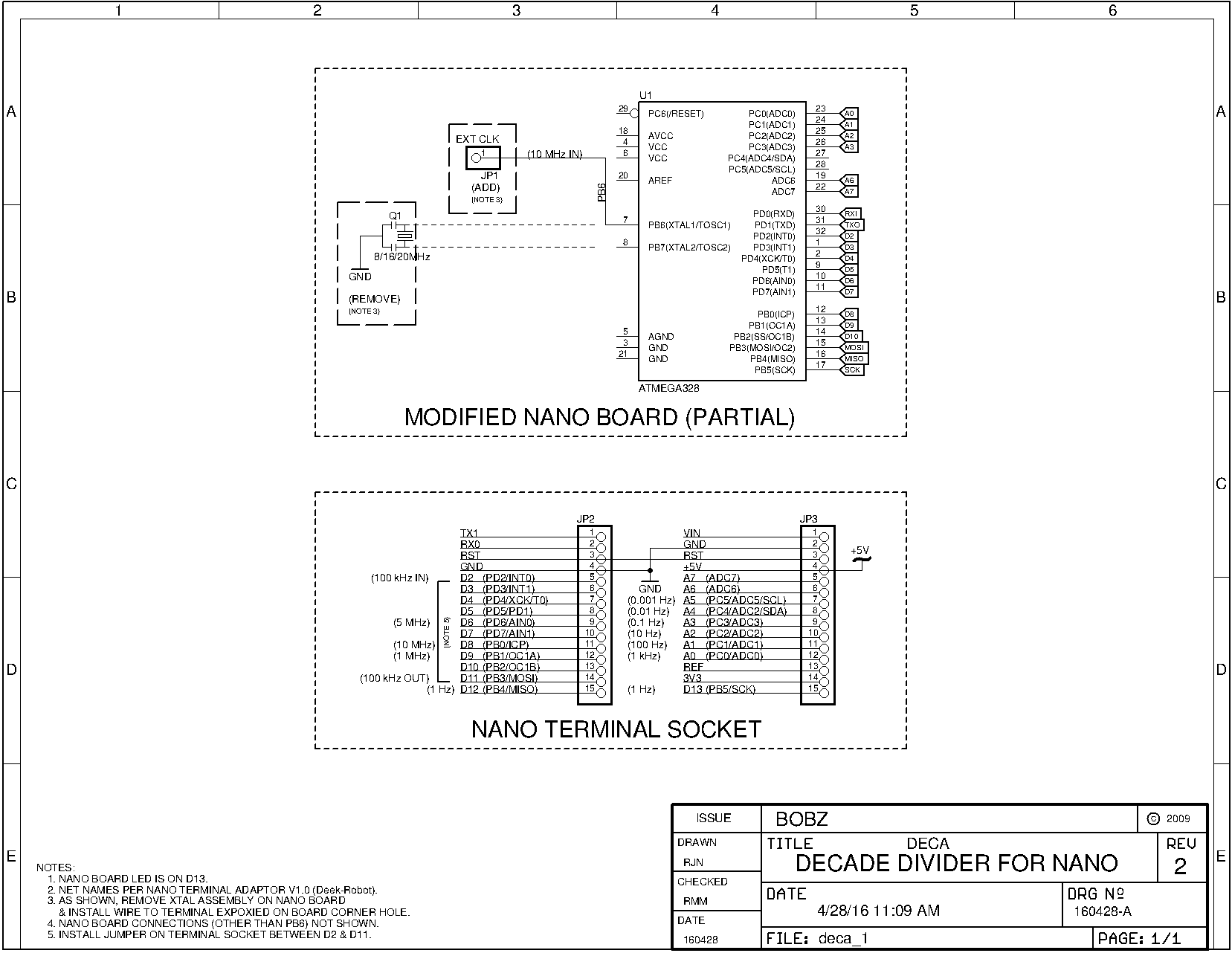
Schematic 1 shows the board rewiring and the clock divisors available at the NANO pins.
The custom hardware modifications consist of removing the NANO's on-board crystal and connecting a wire to an external clock pin. The modifications are detailed in a later section.
Custom NANO software modifications also include reprogramming the NANO's fuse bits for an external clock and for echoing the external clock input to an output pin.
Although the DECA board can be programmed using the hardware-modified NANO operating from an external 10 MHz clock, it is more convenient for initial startup to program the NANO before performing any fuse or hardware changes.
First verify that the NANO is working properly without any modifications. To do this, plug in the USBtiny programmer to the 2x6 programming pins on one end of the NANO and verify that the on-board LED blinks once at startup (the default for some boards is to start up with the LED blinking). Of course, the power LED (usually green) should light to indicate that the board is powered.
To program the target NANO, connect it to a USBtiny hardware programmer and use the chip.bin binary image file to program the board using the d programming script in the DECA application directory (e.g., in the ~/myforth-arduino/rjn/328/deca directory). The programming command line is: sudo ./d. The programming script is given in Figure 1 below.
   #!/bin/bash
   #
   # d command for myforth arduino 160227rjn
   # select either the SPI or bootloader serial downloader
   # eliminate "-B1" from the command line for slow clocks
   #
   set -x

   # on-board bootloader programmer
   # avrdude -p m328p -c avrisp -P /dev/ttyUSB0 -b 57600 -F -U flash:w:chip.bin

   # SPI usbtiny programmer
   # avrdude -c usbtiny -B1 -p m328p -F -U flash:w:chip.bin
   avrdude -c usbtiny -p m328p -F -U flash:w:chip.bin
Figure 1. DECA Programming Script
For the target NANO to function as a DECA, the fuse bytes must be programmed for an external clock and for the clock to be echoed to an output pin (D8 or PB0).
After programming the NANO, use the xclock script in the dude application directory to program the required fuse bits. Note that this programming requires the USBtiny hardware programmer. Also note that after the fuse bytes are reprogrammed, the fuse bytes cannot be read back because the NANO expects an external clock.
The the dude directory is typically maintained in a directory under the current myforth-arduino release such as ~/myforth-arduino/rjn/328/dude. The programming command line is: sudo ./xclock. Figure 2 below shows the fuse programming script.
   #!/bin/bash
   # xclock -- set fuse bits for external clock on XTAL1 -- 160122 rjn
   # also sets fuse bit for clock echo on PB0 -- 160131rjn
   set -x
   wfuse=" lfuse write: 0xb0 "
   dsep="====="

   # must use usbtiny programmer!

   # write operation & date header
   echo -n $dsep >> ./fuses.txt
   echo -n " " >> ./fuses.txt
   echo -n $wfuse >> ./fuses.txt
   echo -n " " >> ./fuses.txt
   echo -n $dsep >> ./fuses.txt
   echo -n " " >> ./fuses.txt
   date '+%y%m%d/%T' >> ./fuses.txt

   avrdude -c usbtiny -b1 -p m328p -U lfuse:w:0xb0:m

   echo " " >> ./fuses.txt
   ./read-fuses   # fuse bytes will show as "??" -- no clock
Figure 2. DECA Fuse Programming Script
The following assumes that the user will be modifying an assembled NANO board with all output stake pins installed. It also assumes that the 2x6 stake pin interface for a hardware programmer is installed.
The wiring changes needed to route an external clock to the NANO board consist of the following steps:
With the above wiring changes, the board can be plugged into a standard breadboard and will accept an external 10 MHz clock on the "extra" pin installed at one corner of the board.
Before performing any modifications, make sure that the DECA program has been loaded and that the fuse bytes have been changed, as described in the previous sections.
Prepare to install a stake pin in the empty hole on the corner of the chip. This hole is near the 2x6 programmer connector and on the same side of the board as the crystal.
With the board components facing up and viewing the board from the programming connector end, the empty stake pin hole is to the right of the programming connector. The positioning of the extra pin is also shown in Photo 1 at the lower left corner of the board. It is the pin that has a wire wrap jumper routed to it on the top of the board.
Once the target hole is located, note that you will be installing a stake pin under the hole and epoxying it to the the board. The epoxy is needed to bond the pin carrier to the board and to prevent the stake pin from pushing up when the modified NANO is inserted into a solderless breadboard.
Break off a single stake pin from a header strip and insert it into the end socket pin of a socket designed for a NANO, such as a terminal breakout board, as shown in Photo 1. Install the NANO in the socket so that the added pin peeks through the end hole. On the other end of the socket, board stake pins will hang off the end of the socket (this is ok).
The socket pin should now relatively stable and can be soldered and permanently glued to the NANO board.
Remove the crystal from the NANO board. This can be done by applying heat to the side of the crystal with a soldering gun. You can also use a hot air gun but be careful to shield the reset switch from heat so that its plastic button is not melted. Note that the reset switch was a casualty of this method on the board shown in Photo 1 (oops!). A small metal shield over the switch should help protect the switch.
When the crystal is removed, you should see three SMT pads on the board near the 328p chip.
Prepare a 1 1/4 inch long wire wrap jumper by stripping 1/16 of an inch of insulation from one end and 1/4 inch of insulation from the other end.
Using Photo 1 as a guide, solder the jumper wire from the SMT pad closest to the board edge to the end stake pin. When soldering the 1/16 inch long end to the SMT pad, first pre-tin both the wire end and the SMT pad. The wire end may have to be pre-bent to route the wire easily along the board edge. Holding the jumper in place with some painters' tape can help stabilize the wire when soldering to the SMT pad. Note that the SMT pad connects to pin 7 of the 328p chip.
The 1/4 inch stripped end of the jumper wire can usually be inserted into a wire wrap tool and wrapped around the end stake pin (about 2 turns). The wire can also be crimped to the stake pin with needle nosed pliers. Solder the stake pin and jumper wire solidly together (make sure both the pin and wire are well-covered with solder). The pin shown in Photo 1 is extra long and was made from a long pin that was manually pressed into the stake pin carrier's body. This can provide a convenient test point, but is not necessary.
At this point, the wire jumper for the external clock is complete. Photo 1 shows the jumper held in place with a dab of E6000 glue, but this is not strictly necessary.
The last step in modifying the board is to permanently attach the added stake pin to the NANO board with some epoxy. Almost any epoxy can be used but we use slow-setup (4 to 6 hours) JB Weld marine epoxy and let it set up overnight. The epoxy mixes up gray, which helps to visually track the application of the glue to the board and to its stake pin carrier. With clear epoxies, glue that has strayed to the mounting socket may be missed.
The epoxy can be applied in several stages with the end of a toothpick. The first location to glue is the underside of the board. The new pin carrier and the original end pin's carrier can be glued together and to the underside of the board with a relatively generous amount of epoxy. There is little danger of gluing the pins to the socket and this provides a solid connection between the new pin's carrier, the adjacent pin's carrier and the bottom of the board.
Next, epoxy the new pin and its solder connection to the top of the board. This keeps the pin from pulling out of the pin carrier when the board is removed from a socket.
The last glueing step is the most delicate. Apply a very small amount of epoxy to the the pin carriers for the new pin and the adjacent pin (i.e., the one marked "TX1"). Also epoxy the new pin's carrier to the outside edge of the board. These two operations firmly attach the new pin's carrier plastic to the carrier plastic of the adjacent pin and to the end of the board.
Only a small amount of glue is needed. Apply the glue high up on the pin carriers, near the board, slathering the epoxy on the edge of the board. Do not let the epoxy creep down on the two pin carriers so that the carriers are inadvertently glued to the socket.
This completes the hardware modification. After the epoxy has set overnight, it should be possible to remove the completed DECA board from the socket with the extra clock pin on the end of the board remaining firmly in place.
Further verify the modification by carefully removing the modified NANO from the terminal socket and confirm that it will insert and remove from a solderless breadboard (e.g., the "extra pin" inserts in correct alignment with all of the other pins).
To functionally verify the completed module, first plug it in to the USBtiny programmer to furnish it with 5 Volt power. Next, apply a 10 MHz 5-Volt square wave between the new clock pin and a NANO ground. One source of a suitable square wave is the output of a "can type" crystal oscillator.
Note that, for DECA to work properly, an external jumper must be installed between pin D2 and D11, as shown in Schematic 1. This jumper routes the 100 kHz output to an input pin so that it can be counted down for lower frequency outputs.
With power and clock applied and the jumper installed, the user LED on the board should blink at a rate of one Hertz. Outputs on other pins should be as shown in Schematic 1. One quick check is to use a scope to observe the 10 MHz clock echoed on pin D8. This reconstructed clock should be a clean 5 Volt square wave at a frequency of 10 MHz.
DECA was designed to be used with a 10 MHz clock from a high-accuracy source such as a rubidium reference. The DECA module is also used as a module in our DECA-FEBO product that provides divided and multiplied clock outputs based on the output of a rubidium reference.
However, DECA can be used as an inexpensive signal generator by feeding it from a crystal oscillator such as a "can type" crystal oscillator. These oscillators are inexpensive, reasonably accurate and easy to connect to DECA.
Initial Release |
Copyright © 2016, Bob Nash.