Page 2
The following describes the design, construction, operation and use of the DECL (Decade PLL) module. The module has both a Phase Locked Loop (PLL) frequency multiplier and a frequency divider to produce various output frequencies that are based on an input reference frequency. The primary use of the module is to condition the ten megahertz (10 MHz) signal from a reference oscillator and produce divided and multiplied outputs synchronized to the reference.
The DECL module uses two chips, a PLL chip and a microprocessor chip, to convert the rubidium input signal to a logic level and multiply and divide that signal to provide multiple frequency outputs that are related to the reference.
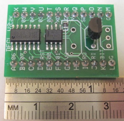
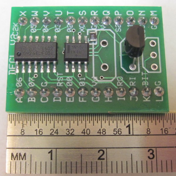
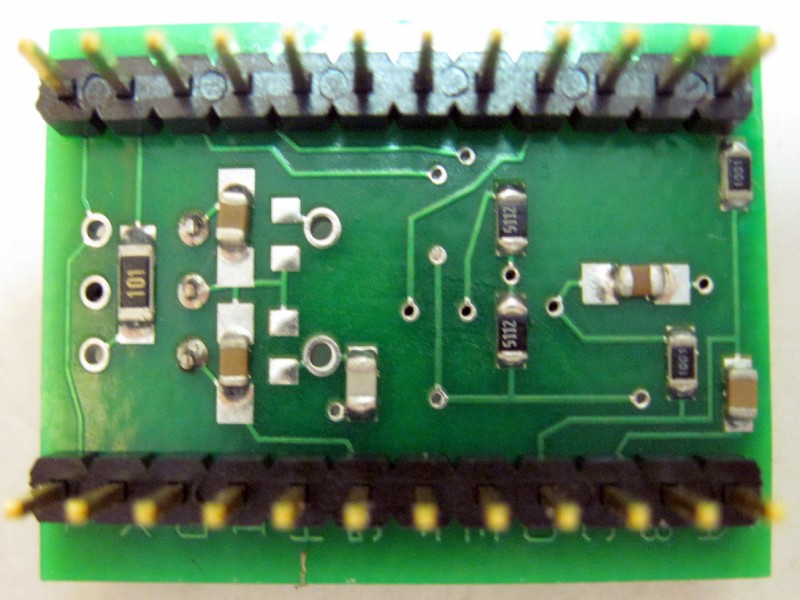
Photo 1 shows a top view of the module and Photo 2 shows the bottom view.
The PLL chip conditions the input signal to provide a buffered, logic-level output. This output also drives the microprocessor clock input. The PLL provides a multiplied output, typically 25 MHz, for use as a stable phase-locked output that is derived from the input reference frequency.
The microprocessor takes the buffered output of the reference signal and divides it to produce marker signals at various frequencies from 1 MHz to 1 Hertz. The microprocessor and its code are the same as used for the DECUS decade divider module.
Page 3
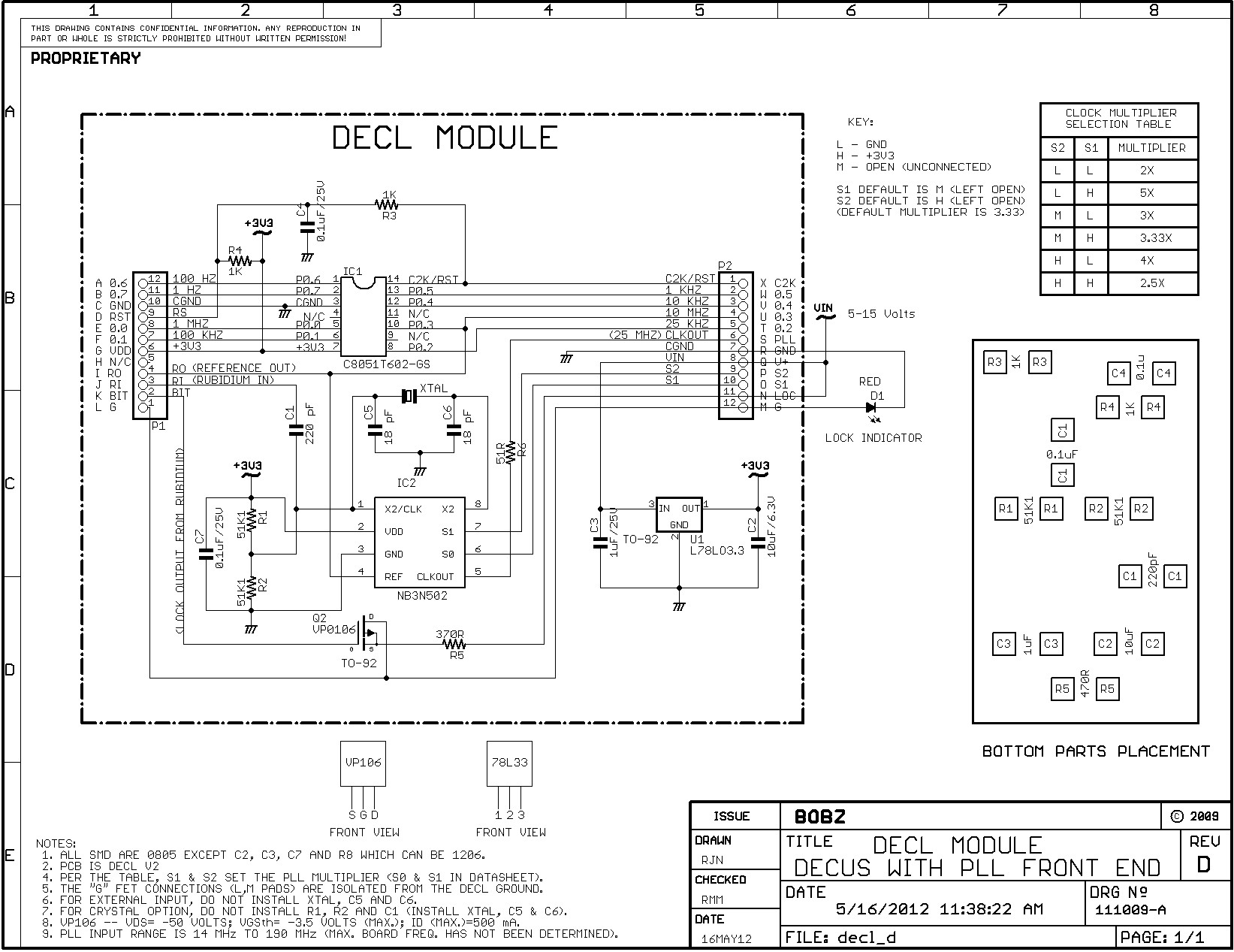
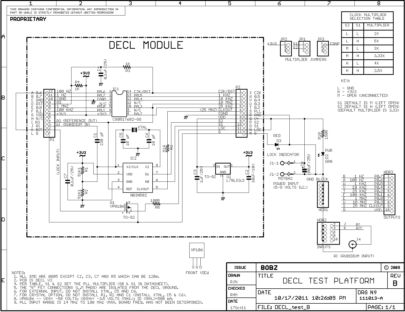
For the following, refer to the Schematic 1 titled "DECL MODULE -- DECUS WITH PLL FRONT END."
You can also download DECL schematics in a zip file.
The schematic shows the components, circuitry and some operational information for the module. For example, the schematic includes a table for PLL jumper options and bottom-side component placement for the DECL PC Board. The Parts List provides additional information about the components used to assemble the module.
As shown in Photo 1, the module measures approximately 1 1/4 by 7/8 inches (32 by 23 mm). This is the same size as the the DECUS module. Signal connections are provided on two 12-pin single-row pin headers. The header connections are labeled "A" to "X" for easy reference.
The connections are also labeled according to function (e.g., "06" for P0.6). Header pins are spaced one tenth of an inch apart and the header rows are spaced 0.6 inch apart. This allows the module to be used with breadboard sockets or wired with in-line sockets on a prototyping board. Note that the inter-pin capacitance of breadboarding sockets can distort some higher frequency outputs, especially PLL outputs with higher multipliers (e.g., 5).
The module provides nine different divider outputs, ranging from one Hertz to one megahertz (MHz). The module also provides a 10 MHz conditioned output and a frequency-multiplied outptut from the PLL chip. The multiplied output is 33.33 MHz when the option pins are left open (factory default). Users will typically want to wire option pins "O" and "P" high to produce a 25 MHz reference output.
With a 10 MHz input from a frequency reference, the multiplied output can range from 20 MHz (2X) to 50 MHz (5X) by wiring the option pins "O" and "P" according to the PLL Multiplier table in the schematic.
The DECL module includes a footprint for a P-channel MOSFET that can be wired to drive an LED. For example this can be used to indicate that a rubidium reference source is locked. As shown in Schematic 1, the LED drive connects to the MOSFET gate at module pin "K" (BIT) and the indicator LED connects between module pin "M" and ground (in "R"). Pin "N" (LOC) must also be wired to the power supply input voltage.
A footprint for a LED current limit resistor, R5, is provided on the module. This is typically 180 Ohms to provide approximately 10 milliamperes through a red LED (assuming a 5 Volt module input). The location of this resistor is marked on the schematic's component placement diagram so that it can be easily identified and adjusted.
The divider outputs are driven by microprocessor port pins capable of sourcing or sinking up to 100 milliamperes (100 mA) each. Thus, the one Hertz output can directly drive an LED to act as an "active" indicator. These drive capabilities are limited by the choice of input voltage and the current limitations of the regulator, as noted in the Power section. The output of the PLL can drive up to 25 milliamperes, also subject to the limitations of the voltage regulator.
Page 4
The input conditioning circuit was developed by experimenting with the input conditioning used for DECUS. The clock input to the PLL was biased to 50% of the supply voltage and capacitively coupled to the input signal from the rubidium oscillator. This approach works but requires a somewhat larger coupling capacitor than used for DECUS.
The input circuit was verified to work reliably with the typical input from an LPRO rubidium reference, which is approximately 0.55 Volts RMS. However, when tested with a variety of rubidium references, some did not provide sufficient output to reliably run DECL. Thus, DECL is sold only as a "frequency reference" module and not guaranteed to work with the outputs of all rubidium reference oscillators.
Our tests show that the circuit works reliably with inputs ranging from one Volt peak-to-peak (p-p) to several Volts p-p. The input was not rigorously characterized versus frequency, but appears to operate reliably in the range of 5 to 20 MHz.
All of the divider outputs are driven by a microprocessor with hardware divider capabilities. Outputs above 10 kHz are derived directly from hardware counters. Thus, these outputs are synchronized with each other and do not depend on software timing loops. Outputs at 10 kHz and below, although generated by software within a timer interrupt routine, are coded so that the outputs are also syncronized. Observing the outputs on an oscilloscope shows reliable synchronization on signal edges.
The module is designed so that all pins are on 0.1 inch centers to facilitate protoboard wiring or plugging into a breadboard socket. If used with a breadboard socket, note that higher frequency signals may be degraded by capacitance between breadboard socket rows. This is especially true for higher frequency PLL outputs.
To set up the module for operation, it is necessary only to supply it with power and an input signal. Once set up for operation, outputs are continuously available at the lettered output pins, as indicated in Schematic 1.
The following sections describe power and signal requirements, module connections and test procedures.
Page 5
All module outputs are tested before shipment with an LPRO-101 or FRS input source with verified signal levels. Outputs are checked for waveform integrity, level and frequency with a Tektronix TDS 2014 oscilloscope.
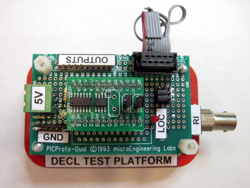
Photo 3 shows the DECL test platform used to test DECL modules.
Like the AGEN test platform, the base is made with a weighted breath mint tin. The tin is filled with junk hardware and coated on the bottom with E6000 glue to make a heavy, slide-resistant base. The test platform circuitry is wired on a protoboard originally designed for microprocessor development. The protobard was trimmed to fit the base and two mounting holes were drilled to allow mounting the board on standoffs. The board is fastened to the base with four hermaphroditic standoffs. The screw ends of the standoffs face up and the board fits over them. The board is held to the base with nylon standoffs screwed on two of the standoff ends.
Paper labels glued next to major components help identify main features of the platform. For example, the "RI" label on the BNC connector indicates the "reference input" from the oscillator.
As shown in Schematic 2, the test platform brings the outputs to a 10-pin single row header. One pin is dedicated to each of the nine output frequencies. Pin 10 is wired to the input voltage so that it can be checked with a voltmeter or scope. The row of output pins is labeled "outputs" in photo 3. Another row of stake pins provides ground connections for scope and voltmeter probes. Where pin indication in necessary, pin 1 of each connector or row of pins is marked with a dab of white paint.
The input from the rubidium reference is connected via a 2X5 shrouded IDC plug; the mating socket and ribbon cable connects to a chassis-mount BNC connector glued to the base. This provides a solid connection for the BNC-terminated cable from the reference while allowing the board to be disconnected from the base for wiring and modifications.
A polarized power connector (labeled "5V") provide 5 Volt power and a green indicator LED (not labeled) provides positive indication that power is applied to the module.
A second red LED connects to the lock indicator P-channel MOSFET as an activity indicator. The FET is driven from the 1 Hertz output so that the red LED flashes when the output is active. This also provides a positive indication that the input signal is present and that the lock indicator FET and the its current limiter are wired correctly.
A table of jumper settings for various multiplication options was cut from the test platform schematic and pasted on the base (not visible) to provide a convenient reference during testing.
Page 6
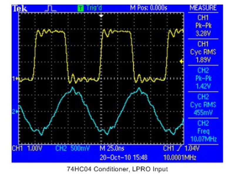
The input signal is applied between the module pins labeled "J" (RI) and "C" (ground), as shown in Schematic 1. The conditioning circuit is designed to be compatible with the LPRO-101 specifications with a typical input signal of 0.55 Volts RMS (approximately 1.5 Volts p-p). DECUS Photo 1 shows the typical input conditioning signals for a LPRO input.
Note: The input may not operate reliably for signal inputs under one Volt peak to peak. Inputs as high as 6 Volts peak to peak have been used but are not recommended for routine operation.
To verify the correct operation of the conditioning circuit, use an oscilloscope to observe the input signal between ground and pin "U" (0.3) of the module. If the input voltage is within the range specified above, a 10 MHz square wave should be present. Also, with no jumpers installed at pins "O" and "P", a 33.33 MHz signal should appear at pin "S" (PLL).
Page 7
The DECL output frequencies and module pins are:
| S (PLL) | 20 - 50 Megahertz (depending on PLL jumper settings) |
| U (0.3) | 10 Megahertz |
| E (0.0) | 1 Megahertz |
| F (0.1) | 100 Kilohertz |
| T (0.2) | 25 Kilohertz |
| V (0.4) | 10 Kilohertz |
| W (0.5) | 1 Kilohertz |
| A (0.6) | 100 Hertz |
| B (0.7) | 1 Hertz |
Page 8
![]()
An on-board 3.3 Volt regulator provides stable regulated power to the module. As shipped the module operates with power inputs from 5 to 16 Volts (assembled modules are verified at 5 Volts). To configure the module for operation, connect power between pin "Q" (VIN) and pin "R" to ground.
Unlike the DECUS module, there is no zener diode on the module for use with higher voltage inputs such as a 19 to 24 Volt source powering an LPRO or FRS rubidium reference. However, two 9.1 Volt, one-watt zeners are furnished with each module. One or two of these can be connected in series with the module's power input to allow it to be used with the 19-24 Volt rubidium supply.
Once the proper input voltage has been selected and configured, the operation of the regulator can be verified by measuring the voltage betweeen ground (pin "C" or pin "R") and the the regulator output (pin "G"). The measured voltage should be within a tenth of a Volt of 3.3 Volts. If the regulator is hot or the output voltage is not within specification, it is likely that the input voltage is too high or too low.
Although the regulator's nominal output voltage is 3.3 Volts, we have seen outputs as low as 3.2 and as high as 3.4 Volts.
The datasheet specifies a worst case minimum input voltage of 5.5 Volts and a typical (not maximum) dropout voltage of 1.7 volts. Because the modules are tested with a supply that measures 5 Volts, operation at this voltage is assured. But, operation at lower voltages is not guaranteed. If there appears to be a problem with operation, measure the module input voltage to see if it may be lower than 5 Volts and also verify the correct operation of the output of the 78L33 regulator. We have not had any modules fail to operate correctly in the field.
The maximum input voltage to the 78L33 is specified as 16 Volts. This specification varies between manufacturers, with some specifying the maximum input voltage as high as 30 Volts (e.g., STmicroelectronics). If your application requires the replacement of the regulator, correct operation of the module should be verified after its replacement.
Page 9
Note that any drive current supplied by the outputs adds to the regulator current and thus increases total dissipation. Operation at 5 Volts provides more than 50 milliamperes of drive for the outputs while maintaining an adequate dissipation margin.
For operation at higher input voltages, such as 24 Volts with two series connected 9.1 Volt zeners, total output buffering current is limited to approximately 20 milliamperes. Operation with a lower supply voltage is recommended to reduce regulator stress and improve output current drive.
The maximum regulator dissipation is 250 milliwatts and the maximum regulator output is 100 milliamperes. The regulator is both current and temperature limited in the event of output overload.
Because the module's quiescent current draw is approximately 30 milliamperes, the input voltage must be limited so that the 250 milliwatt maximum dissipation is not exceeded. Also, the maximum regulator output is 100 milliamperes. The regulator is both current and temperature limited in the event of output overload (e.g., due to higher input voltage or output loading).
With a 9 Volt input the dissipation is: [(9)-(3.3)] Volts X 30 milliamperes = 171 milliwatts. This leaves very little dissipation margin. Thus, it is recommended that the input be supplied from a 5 Volt regulator or limted to a maximum of 9 Volts. With a 24 Volt supply and two series-connected 9.1 Volt zeners, the input to the module is approximately 5.8 Volts (almost ideal). For inputs between 15 and 19 Volts, only use one 9.1 Volt zener in series with the module input.
Page 10
| Part | |||||
| R1,2 | RES, 51.1K, 1/10W, 1%, 0805 | Digikey | 541-51.1KCCT-ND |
||
| R3,4 | RES, 1K, 1/10W, 1%, 0805 | Digikey | 541-1.00KCCT-ND |
||
| R5 | RES, 0R, 1/10W, 1%, 0805 | Digikey | P0.0GCT-ND |
||
| R6 | RES, 51R, 1/10W, 1%, 0805 | Digikey | 541-51.0CCT-ND |
||
| R7 | RES, 470R, 1/10W, 1%, 0805 | Digikey | P470CCCT-ND |
||
| C1 | CAP, 100 pF, 200 Volt, NPO, 0805 | N/A | stock |
||
| C2 | CAP, 10 uF, 6.3 Volt, X5R, 0805 | Digikey | PCC2225CT-ND |
||
| C3 | CAP, 1uF, 25 Volt, X5R, 0805 | Digikey | PCC2319CT-ND |
||
| C4,7 | CAP, 0.1 uF, 50 Volt, 5%, X7R, 0805 | Digikey | 478-3352-1-ND |
||
| C5, C6 | CAP, MLCC, 18 pF, 50 Volt, 5%, COG/NPO, 0805 | Mouser | 140-CC501N180J-RC |
||
| D1 | diode, zener, 1N4739, 9.1 Volt, 1 Watt, DO41 | Digikey | 1N4739ADICT-ND |
||
| D1 | REG, voltage regulator, 3.3 Volt, TO-92, 100 mA, 250 mW | L78L33 |
|||
| IC1 | microprocessor, C8051T602-GS OTP, pre-programmed | Digikey | 336-1655-5-ND |
||
| IC2 | PLL, NB3N502 | Mouser | 863-NB3N502DG |
Page 11
| PCB1 | PCB, DECL V2 | ||||
| PHD1,2 | 12-pin header, SIL, breakaway | FRY'S | PLS-40S-P5 |
Page 12
Original circuit, board revision set at "V2" |