
Page 2
Page 3
The following describes the design, construction, operation and use of the YACC2 and YACC3 crystal calibrators, as described by Bob Miller in the September 2011 issue of QST magazine. The primary use of the modules is to generate crystal-controlled marker signals. For example, the signal outputs can be used for calibrating older HAM Radio receivers or newer home-brew equipment. For a more detailed description of the YACC modules and their applications, refer to the QST article.
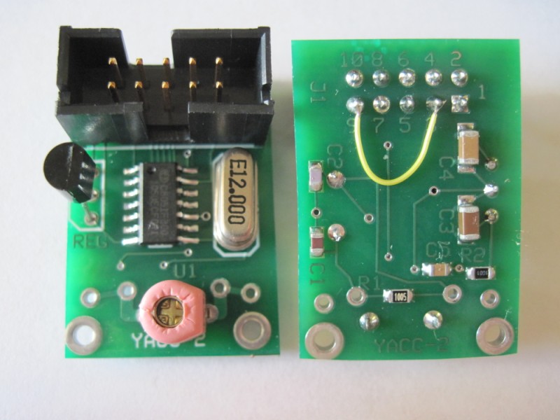
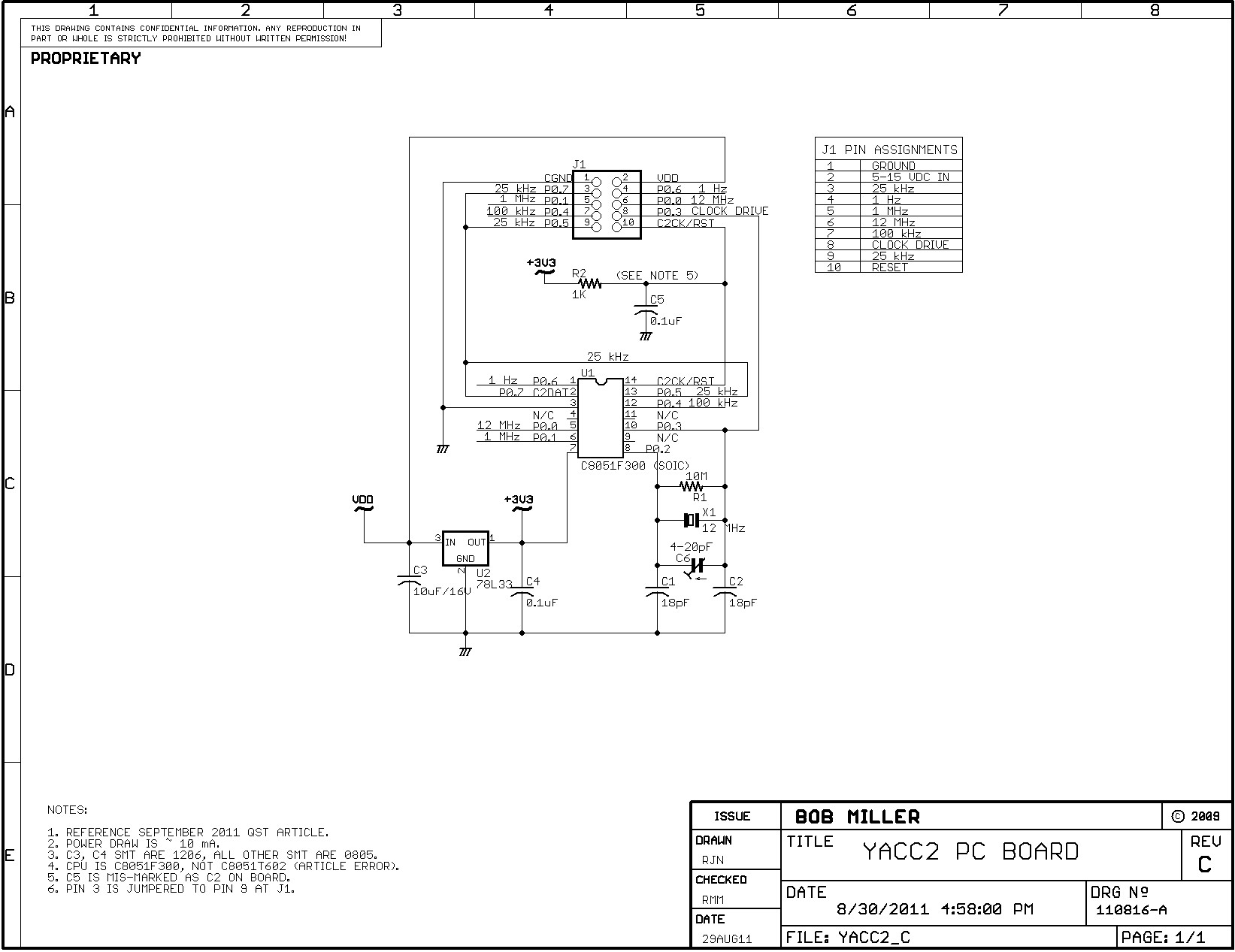
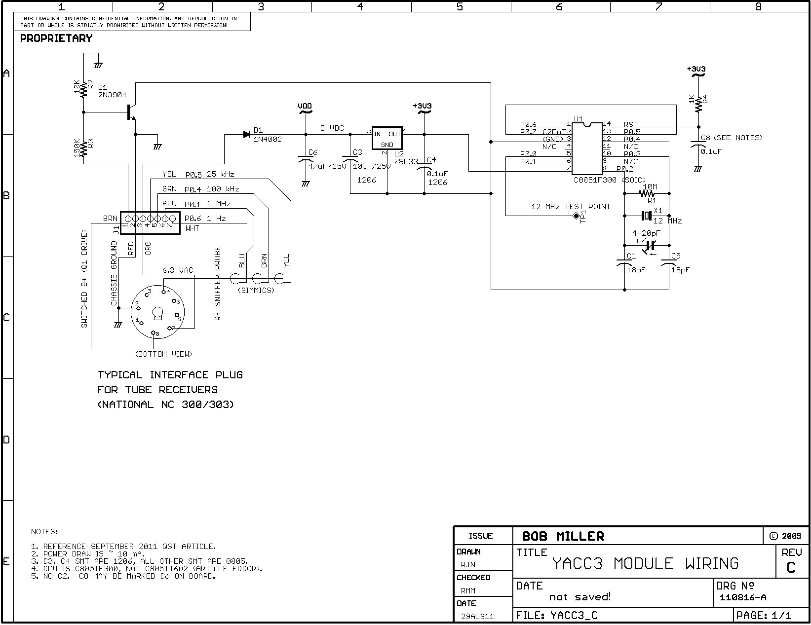
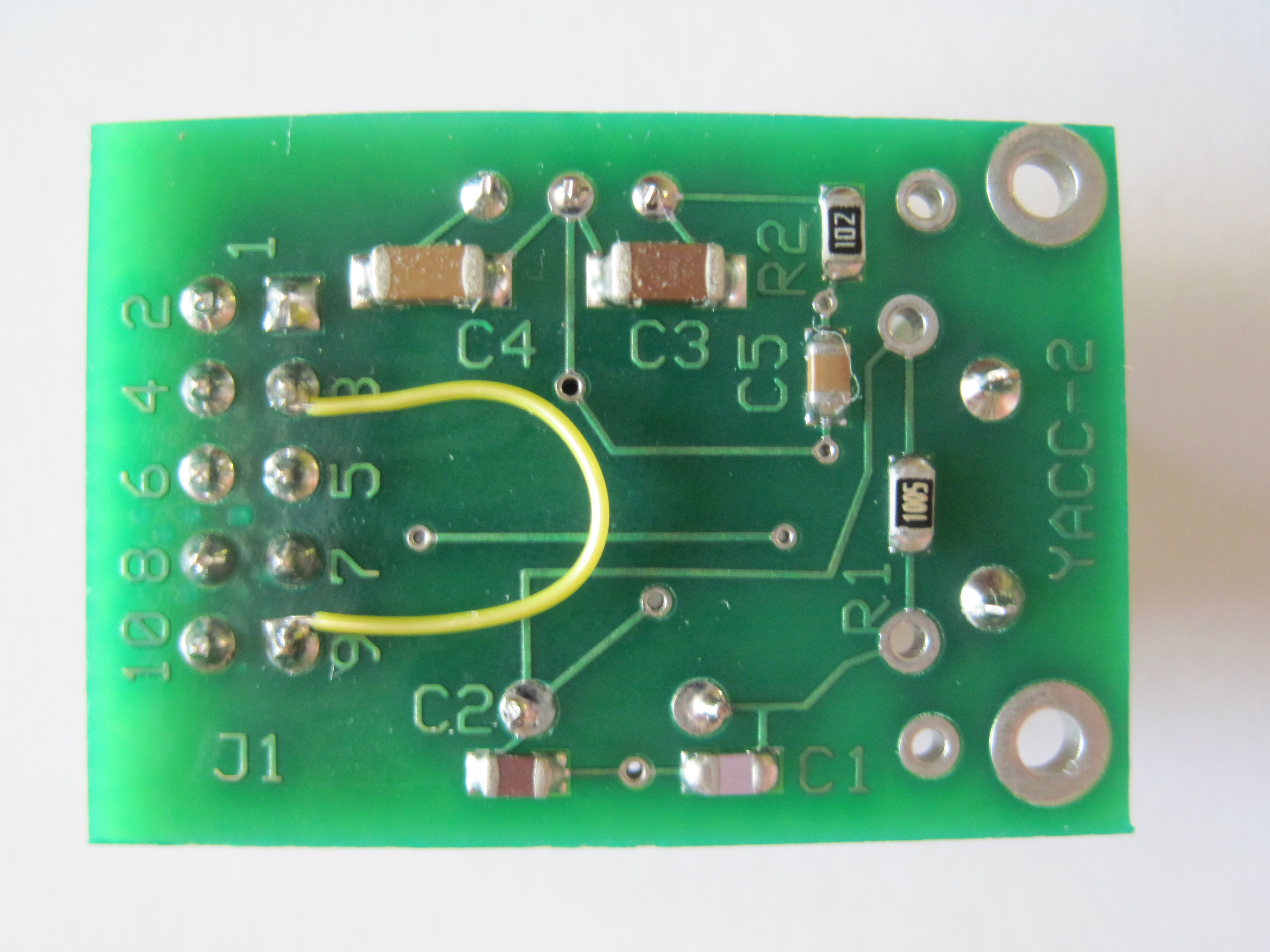
TheYACC2 module has a 10-pin IDC connector for its interface and is intended for standalone use. TheYACC3 module has a single row of 0.1" spaced pads as its interface and is intended for other applications such as mounting inside a tube-based relay case for plugging into the calibrator socket on older receivers.
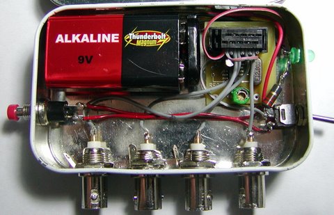
Photo 4 shows the YACC2 module built for standalone use and mounted inside a small breath-mint tin by one of our customers.
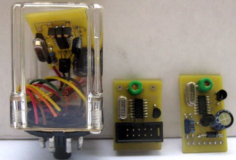
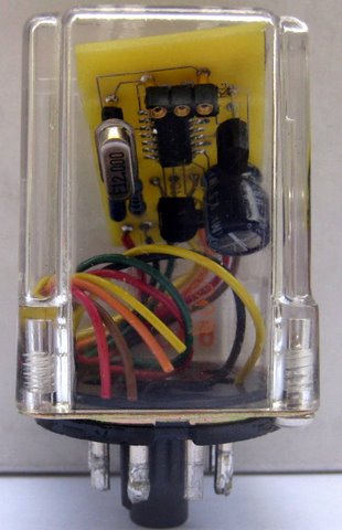
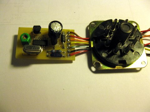
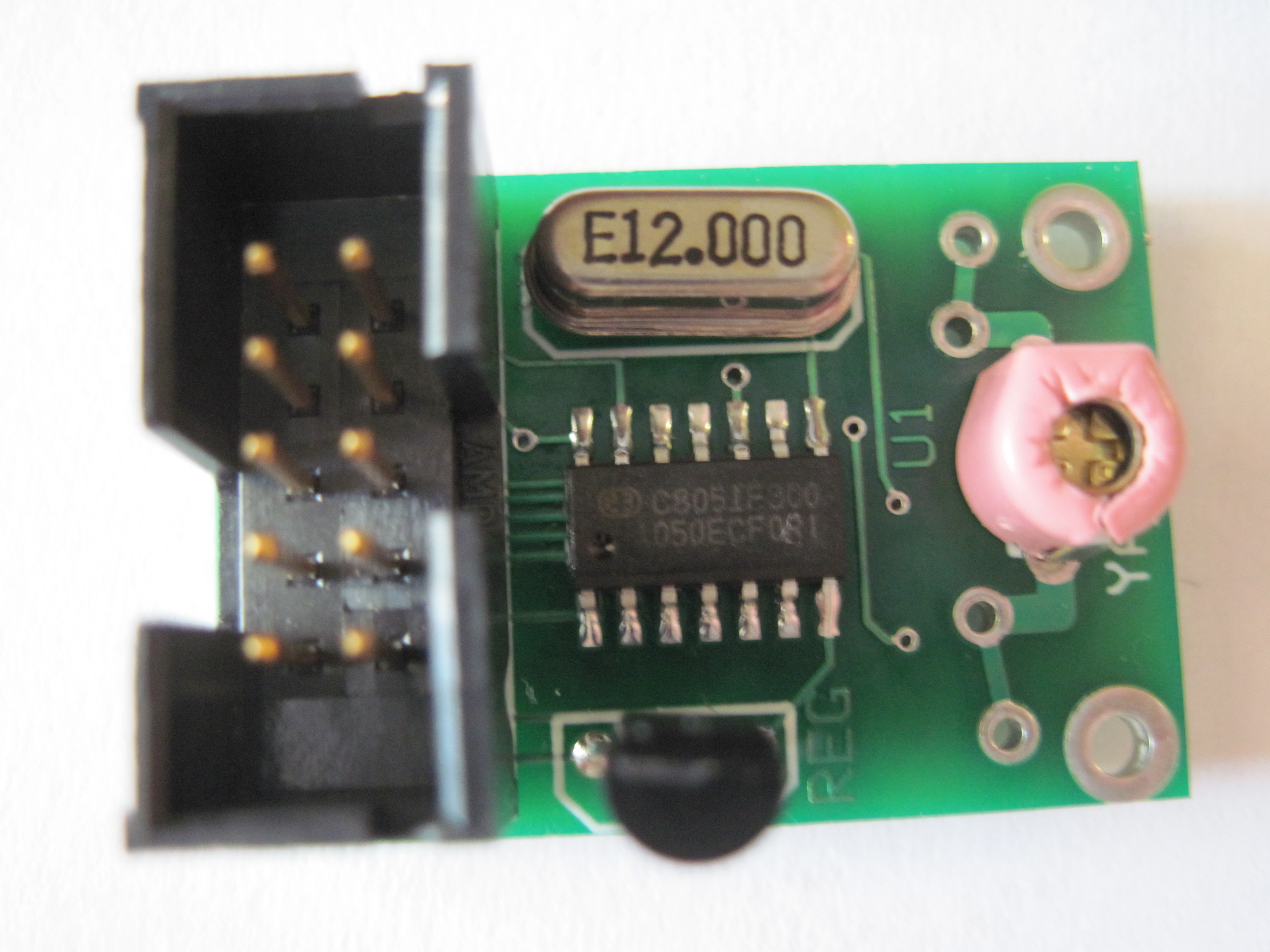
Photo 5 shows the YACC3 module mounted inside a relay case and Photo 6 shows the YACC3 module before being wired to its plug-in base.
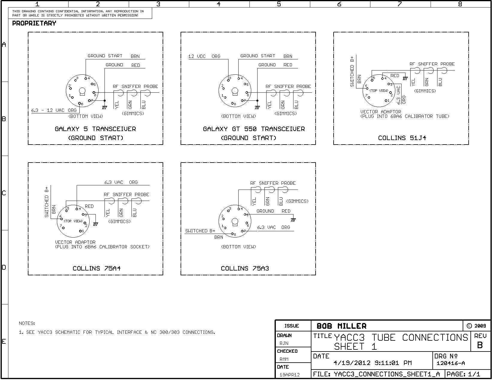
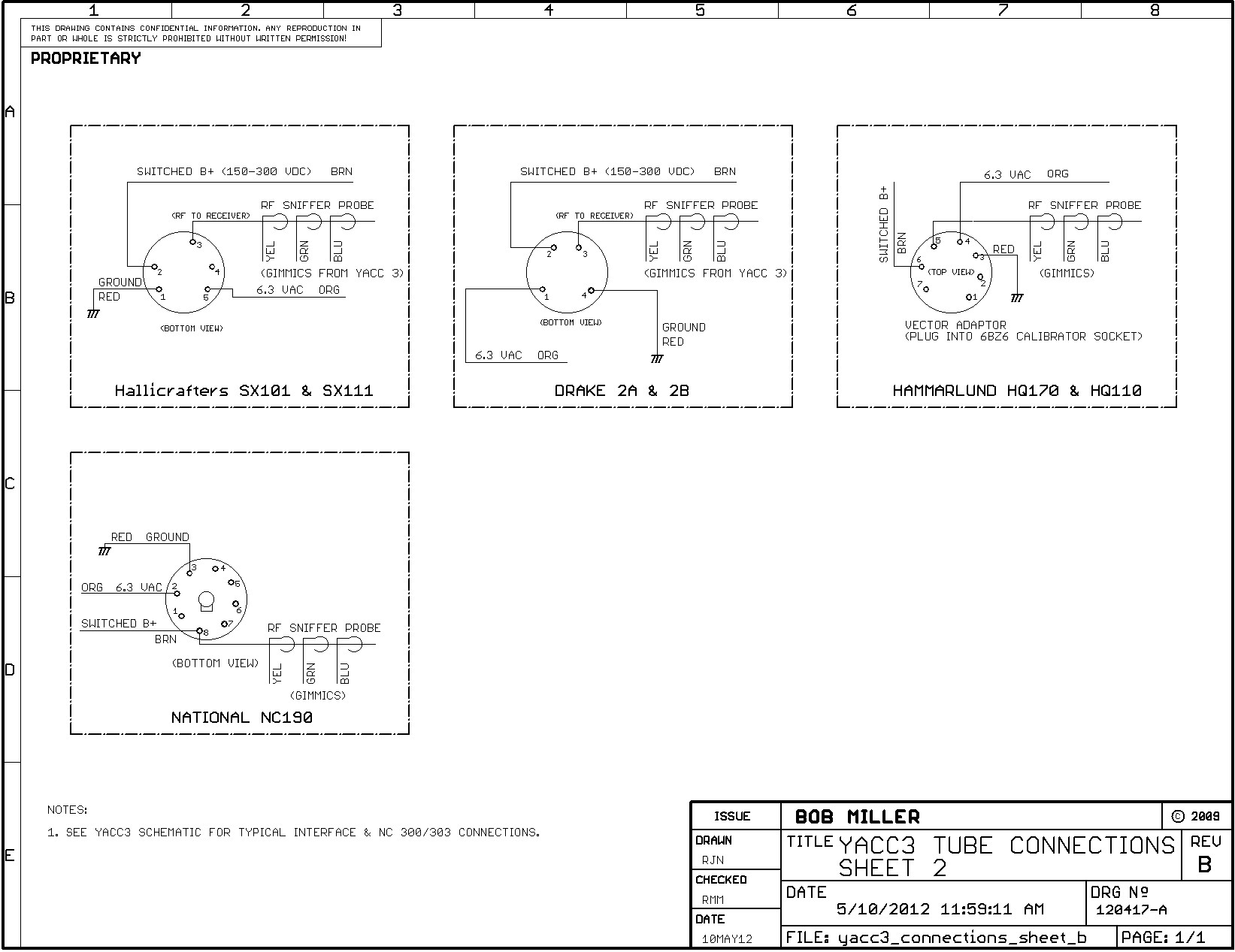
Module wiring is shown in the Schematic 1 (YACC2) and Schematic 2 (YACC3). Receiver plug wiring for the YACC3 module are shown in Schematic 1 and in Schematic 3 and Schematic 4.
You can download Schematics 1, 2, 3 and 4 as a zip file.
Note that some of the photos and schematics are the same as those contained in the article. The schematics given herein have been corrected, however, according to later notes from the author. In particular, the processors are shown as C8051F300s instead of C8051T602s and pin 8 of the YACC2 connector is shown connected to pin P0.2 of the processor instead of ground. Board photos may also be of the newer YACC boards with silk screen and solder mask.
For the following, refer to the schematics and photos given in the previous section. The Parts List provides additional information about the components used to assemble the modules.
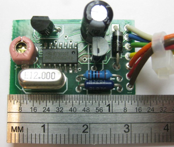
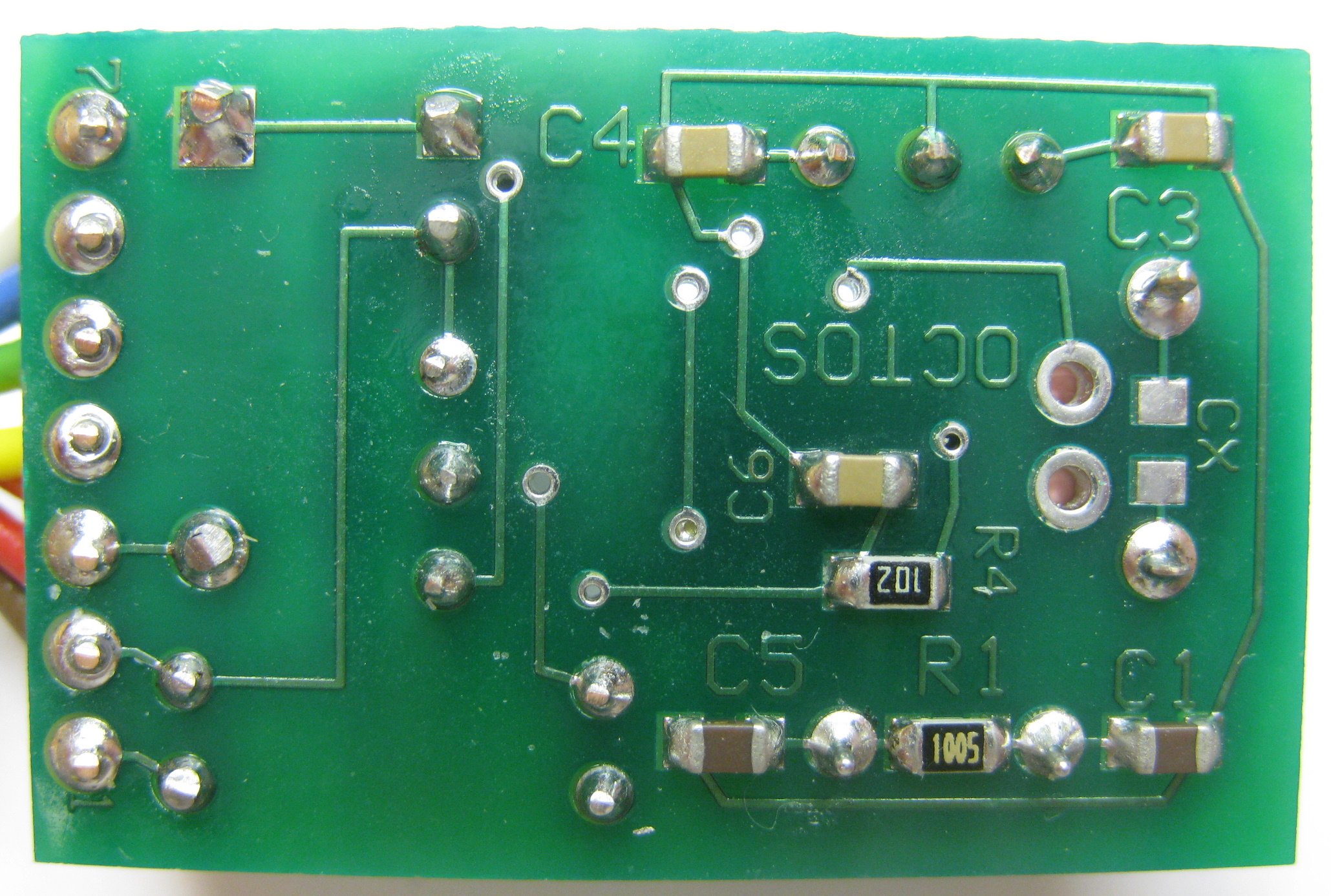
The circuit boards for the YACC2 and YACC3 modules are roughly the same size, measuring approximately 1 1/4 inches by 7/8 inch (32 mm by 23 mm). Photo 3 shows the YACC3 board next to an English/metric scale.
As shown in the YACC2 Schematic, the YACC2 signal connections are available on a 2 by 5 IDC header. As shown in the YACC3 Schematic, the YACC3 signal connections are available on a single row of 0.1 inch spaced solder pads. The YACC3 schematic also shows how the seven connections connect to an octal socket that plugs into the crystal calibrator socket for a NC-300/303.
Page 4
The YACC2 output frequencies at the J1 header pins are:
| 1 | Ground |
| 2 | 5-15 VDC IN |
| 3 | 25 Kilohertz |
| 4 | 1 Hertz |
| 5 | 1 Megahertz |
| 6 | 12 Megahertz |
| 7 | 100 Kilohertz |
| 8 | Clock Drive |
| 9 | 25 Kilohertz |
10 |
Reset |
The YACC3 outputs at the J1 pads are:
| 1 | Switched B+ (Q1 Drive) |
| 2 | Receiver chassis ground |
| 3 | 6.3 Volts A.C. (e.g., receiver filament supply) |
| 4 | 25 Kilohertz |
| 5 | 100 Kilohertz |
| 6 | 1 Megahertz |
| 7 | 1 Hertz |
Page 5
Both modules are normally shipped assembled and tested. However, some customers prefer kit versions. For these customers, boards are shipped with SMT components pre-mounted to avoid difficulty in packaging, identifying and placing small parts.
Partial kits can be easily assembled by examining the top and bottom views of the boards: YACC2 Top View, YACC2 Bottom View, YACC3 Top View, YACC3 Bottom View. For each of the boards, there are a few potential pitfalls. These are discussed in the sections below.
The most probable source of errors for the YACC2 are the backwards installation of the header or the regulator. Most shrouded headers have pin 1 marked on the outside with a small triangle. This must match the square pin on the YACC2 board.
If the connector is installed backwards, connections can be corrected when the cable is assembled. For pre-assembled cables, the wire for pin 1 is normally marked with a red stripe or, for color-coded cables, the pin 1 wire is usually brown. If pre-assembled cables are used, we suggest careful verification of each wire with an ohmmeter before cable connections are finalized.
As for backwards installation of the regulator, its orientation should agree exactly with the silk screen and photo. Note that the 78L33 regulator pinout is reversed from that of most 3-pin regulators: when the regulator is facing you, the input pin is on the right and the output is on the left.
The most common error on the YACC3 board is the incorrect installation of the the regulator at the transistor's position. Note that the regulator is installed near the trimmer capacitor and the transistor is installed near the electrolytic capacitor and rectifier. The correct orientation of the transistor is also important: ensure that the flat side of the transistor body is aligned near the flat side marked on the silk screen.
Another error is inadvertent swapping of the two leaded resistors. The 150K, 1 percent high voltage dropping resistor should be installed nearest the board edge (as marked on the silk screen).
Finally, ensure that the rectifier diode, D1, is oriented with the cathode (silver-banded end) facing toward the board edge -- the banded end solders to the square hole.
Page 6
The YACC2 module was designed for standalone use. Because of its general purpose application, its connections appear at a 2 by 5 shrouded IDC header so that it can be connected with a commonly-available 10-conductor ribbon cable and socket assembly.
The YACC3 module was designed to be connected to pins of an octal-socketed plastic case and installed inside older tube-type radio receivers. This type of installation requires direct wire connections. The YACC3 can also be used for applications where direct wire connections are prefered.
Both the YACC2 and YACC3 modules have on-board regulators to ensure that their circuitry has a stable, regulated supply that can operate from a wide range of voltages. The YACC3 module also has an on-board rectifier diode and filter capacitor to allow it to be powered from the 6.3 Volt A.C. filament supply of a tube radio. The Power section provides more information on module power inputs and connections.
To set up the YACC2 module for operation, it is necessary only to supply it with power. The YACC3 module must also be supplied with a switching voltage before it can operate. When operating, both units provide simultaneous square wave outputs at a variety of frequencies, as described in the Outputs section.
The output frequencies include the crystal reference frequency of 12 megahertz and the most common marker frequencies of 25 kilohertz and 100 kilohertz. A one-Hertz output, connected to an LED through a dropping restor, can be used to provide operational indication.
Wiring the YACC3 for proper operation depends on the application. If the YACC3 is used with an octal relay socket with an older tube receiver, refer to Bob Miller's article. The YACC3 Schematic shows how to wire the YACC3 for use with NC-300/303 receivers. Note the caution given in the article about receivers using B+ start. Also, be aware that high voltage may appear on the PC board at one end of R3 and on pad 1 at the board edge.
Page 7
Most YACC2 and YACC3 modules are shipped assembled and tested. Testing includes verification of all output frequencies. Startup of the YACC3 modules is also verified by switching the B+ lead. The B+ test voltage is 37 Volts, but the operational voltage can be as high as 250 Volts.
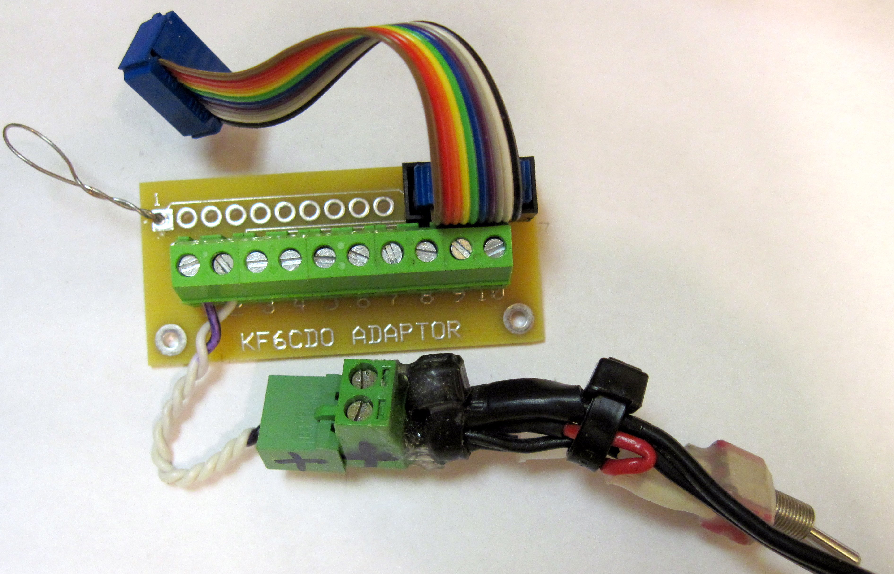
The YACC2 module is tested using the BOBZ1 Breakout Board that breaks out the pins of a 10-pin shrouded IDC connector to a row of 10 screw terminals and a row of 0.156" spaced pads. As shown in the photo, the power is fed to the power input pins of the YACC2 using a polarized connector assembly fed from a 5 Volt wall wart supply. Note that the power connector also has a power switch and indicator LED tie-wrapped near the connector so that power can be switched during testing.
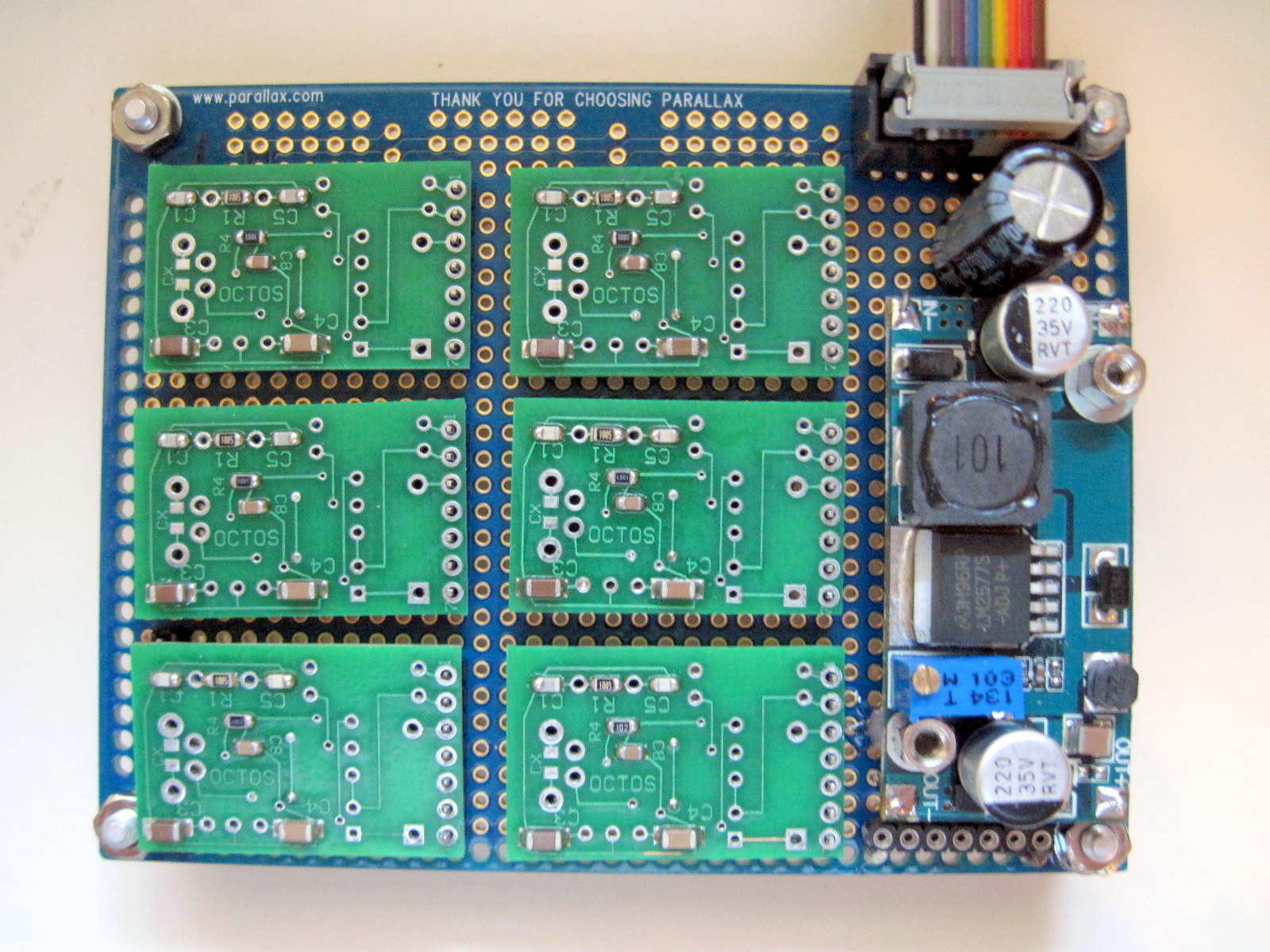
Most YACC3 modules are shipped assembled and tested. Photo 16 shows the assembly and test fixture used for production YACC3 modules. Like many of our projects, the fixture is built on a Parallax proto board. Positions are provided for six boards. These are primarily used for bottom-side SMDs and the processor on the top side of the board. After the SMDs are mounted, the boards are removed from the assembly fixture and through-hole components are mounted by hand using a drill press vice to hold the boards during soldering.
After assembly, color-coded wires are attached to one end of each board. The wires are plugged into a machined-pin connector near the switching power supply at the top of the board. A 9-Volt supply is connected to the board and routed to the YACC3 module's filament supply input. This simulates rectifying 6.3 VAC that is applied to the 3.3 Volt regulator. The switching regulator steps the 9 Volt supply to 27.6 Volts. This voltage is applied to the "B+" input for testing the switching capability of the module.
Some YACC3 modules have been furnished as semi-kits. Although furnishing the YACC3 module as a semi-kit precludes testing, all crystals furnished with the YACC3 kit are tested before shipment. Programming is also verified with the programming checksum displayed by the manufacturer's Integrated Development Environment; critical jump locations are also visually verified on the chip's hexadecimal dump.
Some YACC3 modules are furnished assembled in tube socket bases and wired for specific receivers. All of the YACC3 modules used in these custom assemblies are tested as described above. Additionally, some units are tested by plugging them into sockets on the target receivers. Other assemblies are tested with special test sockets before shipment.
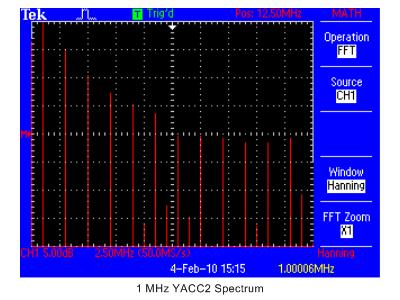
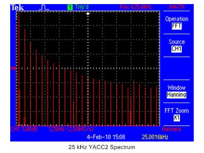
Photo 12 shows the spectrum for a 100 kHz output. Photo 13 and Photo 14 show the spectrum for YACC outputs for 1 MHz and 25 kHz, respectively.
Page 8
![]() The YACC2 and YACC3 modules are not protected against input voltage reversal. Take care to verify that the correct voltage polarity is applied to the power input pins.
The YACC2 and YACC3 modules are not protected against input voltage reversal. Take care to verify that the correct voltage polarity is applied to the power input pins.
An on-board 3.3 Volt regulator provides stable regulated power to the YACC2 and YACC3 modules.
To configure the YACC2 module for operation, connect the negative input of the power supply (i.e., ground reference) to J1 pin 1 (J1/1) and connect the positive supply voltage to J1/2.
The YACC3 (octal-socketed case) module can be operated from the filament supply of a receiver, as shown in Schematic 2. Module connections will vary depending on the type of receiver, as shown in Schematic 3 and Schematic 4.
Note that, allowing for the voltage drop of D1, the YACC3 module can also be powered from a DC voltage. With D1 in place, the YACC3 board should operate for voltage inputs of 5.5 to 16.5 Volts D.C. The unit can operate within the same range as the YACC2 module if D1 is shorted or replaced with a wire. However, operation at a slightly higher voltage with D1 in place is recommended: this protects the module from power supply voltage reversal.
In addition to the voltage required for powering the module, YACC3 requires an external switched voltage to turn the module on and off. This voltage should be in the range of 40 to 250 Volts. The module will switch with a lower voltage range if R3 is reduced. For example, to turn the module on with a voltage of 3.3 Volts, reduce R3 to 4.7K. Also, it is not strictly necessary to install R2 -- it was originally part of an earlier design using an FET for switching. However, its installation is recommended for additional stability and spike protection.
Page 9
The YACC2 (standalone) module operates with power inputs from 5 to 16 Volts.
Once the proper input voltage is applied to the J1 pins, the operation of the YACC2 regulator can be verified by measuring the voltage between ground (J1/1) and the output of the regulator, which is labeled "REG" on the PCB (it also directly connects to pin 7 of the chip, U1). The measured regulator output voltage should be within a tenth of a Volt of 3.3 Volts.
The YACC2 module's quiescent current draw is approximately 12 milliamperes. The current draw of the YACC3 is the same, but the loading is only from the rectified filament supply. The filament supply of the receivers given in the schematics can easily run the YACC3 module.
For both modules, the maximum regulator dissipation is 250 milliwatts and the maximum regulator output is 100 milliamperes. This limit can be challenged by the YACC2 module if the outputs are loaded too heavily. The maximum loading for the chip is approximately 500 milliamperes and 100 milliamperes for any single output. The regulator is both current and temperature limited in the (unlikely) event of output overload but the chip is not protected against overloaded outputs.
Page 10
The following are the parts for the YACC2 module:
| Part | |||||
| R1 | RES, 10M, 1/8W, 1%, 0805 | Digikey | 541-10.0MCCT-ND |
||
| R2 | RES, 1K, 1/8W, 1%, 0805 | Digikey | 541-1.00KCCT-ND |
||
| C1, C2 | CAP, MLCC, 18 pF, 50 Volt, 5%, COG/NPO, 0805 | Mouser | 140-CC501N180J-RC |
||
| C3 | CAP, CERM, 10 uF, 16 Volt, 10%, X7R, 0805 | Stock | N/A |
||
| C4, C5 | CAP, 0.1 uF, 50 Volt, 5%, X7R, 0805 | Digikey | 478-3352-1-ND |
||
| C6 | CAP, trimmer, 4-20 pF, 100 Volt, N450, 0805 | Mouser | 81-TZ03T200E:.69B00 |
||
| U1 | voltage regulator, 3.3 Volt, TO-92, 100 mA, 250 mW | L78L33 |
|||
| U1 | microprocessor, C8051T300-GS, pre-programmed | Digikey | 336-1535-5-ND |
||
| PCB1 | PCB, YACC2 | ||||
| J1 | 2 by 5 header, shrouded | stock | N/A |
||
| X1 | crystal, 12 MHz, HC-49U | stock | N/A |
Page 11
The following are the parts for the YACC3 module:
| Part | |||||
| R1 | RES 10M, 1/8W, 1%, 0805 | Digikey | 541-10.0MCCT-ND |
||
| R2 | RES, 10K, 1/4W, 5%, axial lead | stock | N/A |
||
| R3 | RES, 150K, 1/4W, 1%, axial lead | stock | N/A |
||
| R4 | RES, 1K, 1/8W, 1%, 0805 | Digikey | 541-1.00KCCT-ND |
||
| C1, C5 | CAP, MLCC, 18 pF, 50 Volt, 5%, COG/NPO, 0805 | Mouser | 140-CC501N180J-RC |
||
| C3 | CAP, CERM, 10 uF, 16 Volt, 10%, X7R, 0805 | Digikey | 478-1402-1-ND |
||
| C4, C8 | CAP, 0.1 uF, 50 Volt, 5%, X7R, 0805 | Digikey | 478-3352-1-ND |
||
| C6 | CAP, 47 uF, 25 Volt, 10%, 0805 | stock | N/A |
||
| C7 | CAP, trimmer, 4-20 pF, 100 Volt, N450, 0805 | Mouser | 81-TZ03T200E:.69B00 |
||
| U1 | voltage regulator, 3.3 Volt, TO-92, 100 mA, 250 mW | L78L33 |
|||
| U1 | microprocessor, C8051T300-GS, pre-programmed | Digikey | 336-1535-5-ND |
||
| PCB2 | PCB, YACC3 | ||||
| Q1 | transistor, NPN, 2N3904 | stock | N/A |
||
| X1 | crystal, 12 MHz, HC-49U | stock | N/A |
||
| RC | case, octal socket relay case | stock | N/A |
Page 12
potential QST article. |
||
new board run for QST article demand. Also, Eagle-format schematics and HTML documentation. |
||
new board run for QST article demand. Fixed wire error on YACC2 board. |