The following documents the results of low power tests performed on a C8051F850 (850) processor. For testing, a MINT board was modified to eliminate the 3.3 Volt regulator and the "PWR" indicator LED. The modified board was mounted on a MINT development platform consisting of a socket for the MINT board and screw-down terminals for I/O connections.
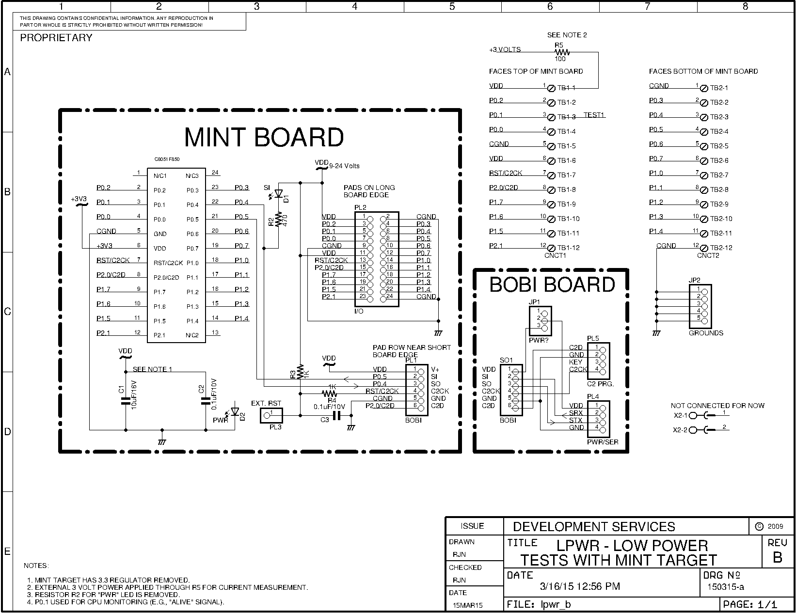
Schematic 1 shows the MINT modifications, development board connections and interface to the BOBI board for programming. Application Note 8 describes the BOBI interface in more detail.
Power consumption was measured by inserting a 100 Ohm resistor in series with the MINT power connection. In Schematic 1 this resistor is designated R5. The actual value of R5, 99.29 Ohms, was measured with an Agilent 34410A multimeter and is used for all calculations.
Page 2
The voltage drop across R5, divided by its value determines the current consumption of the processor. The test voltage was applied to R5 with a BK Precision 9110 adjustable power supply. The voltage was adjusted to as near as possible to 3 Volts.
Because power can feed from the MIDE programmer board to the test board, the BOBI board was disconnected prior to performing all measurements.
Power reduction was performed solely by reducing the 850's clock speed by using the internal low frequency oscillator and further reducing consumption by dividing this oscillator down before being used as the system clock (SYSCLK). Other methods, such as using the idle and stop modes, may result in additional power savings but these are more complicated to implement and were not tried. Analog peripherals, such as the A/D converter and programmable counter array, were disabled for all tests.
To verify that the processor was functional, a port pin was toggled and monitored on an oscilloscope. This signal was generated by a tight "main" loop, as described in the software section below.
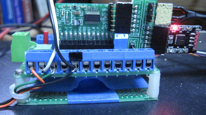
Photo 1 shows the MINT board mounted on a development board and connected to the programmer via a BOBI interface. The instrumentation, MIDE programmer and current measurement resistor are not shown.
Photo 1. Low Power Testing with a MINT Board
Page 3
Figure 1 shows the chip initialization performed to reduce power consumption.
     117	:m -int   [ 7 .IE clr ] m;   :m +int   [ 7 .IE set ] m;
     118	\
     119	-: ?OSCLCN  OSCLCN #@  6 .T if. drop ; then drop ?OSCLCN ;
     120	\
     121	-: /chip  \ initialize chip
     122 \
     123	\ -----[ disable watchdog ]
     124	\
     125	   -int
     126	   $de # WDTCN #!    $ad # WDTCN #!  \ disable watchdog
     127	\
     128	\ -----[ enable LF clock ]
     129	\
     130	   $80 # OSCLCN #!   ?OSCLCN  \ enable LF clock/8, stabilize
     131	\
     132	\ -----[ select clock source ]
     133	\
     134	\   $00 # CLKSEL #!    \ internal 24.5 MHz osc., SYSCLK/1  150315rjn
     135	\   $02 # CLKSEL #!    \  LF clock/8, SYSCLK/1  150315rjn
     136	\   $32 # CLKSEL #!    \ LF clock/8, SYSCLK/8   150315rjn
     137	   $72 # CLKSEL #!   \ LF  clock/8, SYSCLK/128  150315rjn
     138	\
     139	\ -----[ configure I/O ]
     140	\
     141	   $00 # XBR2 #!     \ disable xbr
     142	\   $f0 # ADC0PWR #! \ makes no difference for low power
     143	\ ----- port 0
     144	   $ff # P0MDOUT #!  \ all push/pull outputs
     145	\ ----- port 1
     146	   $ff # P1MDOUT #!  \ all PP outputs
     147	\ ----- port2
     148	   $fe # P2MDOUT #!  \ P2[0] DI -- C2D
     149	   $00 # XBR1 #!        \ no resources routed to port pins (default)
     150	   $40 # XBR2 #!   ;    \ enable XBR, weak pullups
Figure 1. Chip Initialization for Low Power
Page 4
Line 119 defines ?OSCLCN to check that the low frequency clock is stabilized. This is performed by verifying that bit 6 of the OSCLCN register is set. If this bit is not set, the word loops until it is. The initial code for low power operation did not have this check and appeared to work reliably. It was included primarily to be politically correct.
Line 130 sets bit 7 in the OSCLCN register to enable the low power oscillator and then uses ?OSCLCN to check that it is stable before selecting it as a clock source. The lower two bits of OSCLCN set the low frequency clock rate. In this code, the rate is set to the lowest value: divide by 8. Thus, the nominal 80 kHz rate of the low frequency clock is divided down to 10 kHz.
Lines 131 to 137 set the CLKSEL register to select the low frequency internal oscillator and the SYSCLK divisor rate. With the lowest divisor of 128, the SYSCLK rate is approximately (10 kHz)/128 = 78.125 Hertz.
Lines 139 to 150 configure the chip I/O. In this case, most port pins are set to outputs and no system resources are routed to port pins. Note that the system clock can be routed to a port pin (e.g., P0.0) to check the actual clock frequency. This was not done for the low power tests because the frequency could easily be calculated from the period of the output signal and instruction timing.
Figure 2 shows the definition of the word alive that generates the square wave output on P0.1. Note the use of alive in the turnkey startup word, go.
  1	:m alive  [ 1 .p0 toggle ] m;  \ generates "alive" signal
  2  \
  3	-: go  /chip  begin alive again  \ turnkey startup word
Figure 2. Turnkey Startup
Line 1 is a macro that toggles port 0, pin 1.
Line 3 defines the turnkey startup word, go. The startup word first executes /chip to initialize the chip. The initialization word is defined in Figure 1, above. After initialization, the program enters an infinite loop that repeatedly executes alive, defined in Line 1, to toggle P0.1.
The signal on P0.1 is used to show that the processor is operating and to generate a square wave that can be used to determine the system clock rate. The following sections show clock rate calculations.
Page 5
To provide a baseline, the processor was run with the 24.5 MHz internal clock. The alive word was coded as a subroutine and run inside the main loop, as given above in Figure 2, line 3. The power supply was adjusted to 3.001 Volts with no BOBI interface connection. With the BOBI interface disconnected, the output frequency was 9943.4 kHz. Current draw was: (3.001-2.601)/99.28 = 4.02 milliamperes (mA).
The application code was also configured for the standalone interpreter with the main routine running the interpreter word, quit. With no BOBI connection, the current draw was 4.5 mA.
The internal LF oscillator was set for divide by 8 and SYSCLK was set for divide by 1 to generate a 10 kHz clock. With alive coded as a call to toggle P0.1, the output frequency was approximately 481 Hz.
With a 10 kHz clock and alive coded as a macro, the output frequency increased to approximately 1.25 kHz. With this faster coding, the half cycle of the output square wave is around 1/10 millisecond (ms) times the bit toggle time (2 cycles) and the loop jump time (another 2 cycles). Thus, each half cycle of output is about (4)(1/10) ms = 0.4 ms. This was confirmed on the oscilloscope. The current was: (3.0013-2988.0)/99.29 = 133.96 microamperes (uA).
To see if the output pin toggling and scope measurement affected the current draw, alive was replaced with two "nop" instructions. There was no change in the current draw
The LF oscillator was set for divide by 8 and SYSCLK was set for divide by 8 to generate a 1.25 kHz clock (10 kHz divided by 64). With alive coded as a macro, the output frequency was approximately 156.4 Hz (half cycle = 3.2 ms). The time for a half cycle should be (4)(0.8) = 3.2 ms, agreeing with the period observed on the oscilloscope. Current draw was: (3.0012 - 2.9896)/99.29 = 116.83 uA.
With coding the same as for the 1.25 kHz clock, the internal LF oscillator was set for divide by 8 and SYSCLK was set for divide by 128 to generate a 78.125 Hz clock. The output frequency was approximately 19.2 Hz (half cycle =~ 52 ms). Current draw was: (3.0013 - 2.9898)/99.29 = 114.82 uA
Page 6
With the 78.125 MHz clock, the voltage was lowered to 2.7 Volts. Current draw was: (2.7005 - 2.6892)/99.29 = 113.80 uA.
The power supply was also adjusted downward to see what the cutout voltage was for this particular chip. The lowest operational voltage was determined by ensuring that the chip reset and functioned reliably after power cycling. The limit was 2.17 Volts, in good agreement with the 2.2 Volts minimum specified in the datasheet. Note: the datasheet specifies an operational range of 2.2 to 3.6 Volts.
Figure 3 provides a summary of the above test results.
9943.4 |
0.0001 |
4,020 |
HS internal clock, SYSCLK/1, alive=call |
||
9,943.4 |
0.0001 |
4,500 |
HS internal clock, SYSCLK/1, main loop running quit (serial interpreter) |
||
481 |
2.08 |
134.0 |
OSCLCN/8, SYSCLK/1, alive=call |
||
1,250 |
0.8 |
134.0 |
OSCLCN/8, SYSCLK/1, alive=macro -- replaced "alive" with nop, no difference |
||
156.4 |
6.4 |
116.8 |
OSCLCN/8, SYSCLK/8, alive=macro |
||
19.2 |
51.2 |
114.8 |
OSCLCN/8, SYSCLK/128, alive=macro |
||
19.2 |
51.2 |
113.8 |
OSCLCN/8, SYSCLK/128, alive=macro -- this chip operates down to 2.17 Volts |
Figure 3. Summary of Test Results
Page 7
Page 8
Page 9
Initial Release |
Copyright © March 2015, Bob Nash.
Page 10