Page 2
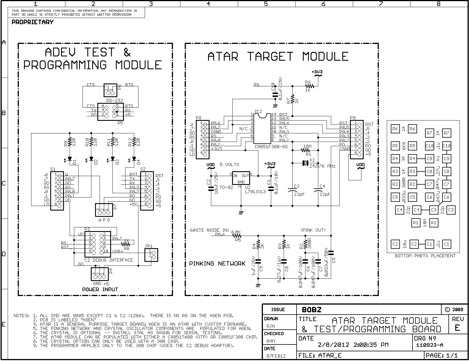
The ADEV Development System consists of the ATAR Target Module and the ADEV Test/Programming Module. The ATAR Target Module and the ADEV Test/Programming Module, together with development tools from Silicon Laboraties, Inc. (SL), can be used to develop custom applications for C8051F300 and C8051T600 processors (300 and 600 chips).
Throughout the remainder of this documentation, the term "ATAR" refers to the ATAR Module and the term "ADEV" refers to the ADEV Test/Programming Module. The term "AGEN" refers to an ATAR Target Module populated and programmed to provide an audio test and generator module (see AGEN Module).
The development system was originally designed to develop code for the AGEN (Audio GENerator) Module described elsewhere in this documentation. The ADEV system is primarily intended for users who want to develop custom firmware for 300 and 600 chips. But, the system can also be used to upgrade or change the firmware on an AGEN audio generator module.
The ATAR Module provides an on-board regulator, a reset circuit and a general-purpose resistor/capacitor (RC) network (on the bottom of the board). All chip pins and regulated power are brought out to two single-row pin headers that are tenth-inch spaced to facilitate easy mounting and breadboarding.
Thus, the ATAR is suitable for projects that require a "ready to use" processor module that supports chip features such as eight I/O pin, an A/D converter, a pulse width modulator, timers and a Programmable Counter Array (PCA).
The ATAR Target Module consists of a target board (labeled "AGEN") populated with either a 300 or a 600 chip. These chips are both available in 14-pin SOIC packages and are pin-compatible. The 600 chip is a One Time Programmable (OTP) version of the 300 chip, but it does not support an external crystal oscillator (there are also some other minor differences).
The ADEV Test/Programming Board accepts an assembled ATAR Module (or AGEN Module) and has facilities such as a serial port interface connector and test LEDs for module testing. In the case of an ATAR populated with a 300 chip, the Test/Programming board can be used to program the chip.
The ATAR populated with a 600 OTP chip provides a pre-programmed Target Module. Note that the OTP 600 chip must be programmed with a special SL programmer before being installed on the ATAR Target Module.
An ATAR populated with a 300 chip provides a programmable Target Module. When using an ATAR populated with a 300 chip, the chip can be programmed with ADEV and the standard SL programming tools (i.e., Debug Adaptor and IDE software).
For example, the SL Debug Adaptor plugs into a 10-pin shrouded connector on the Test/Programming board, allowing a 300 chip to be programmed with the ADEV Module.
As mentioned above, when a 600 chip is used, it must be programmed with a separate SL programmer. However, the Test/Programming platform can still be used to test ATAR modules populated with 600 chips. For example, the ADEV serial interface and LEDs can be used to test 600 chips that use these features.
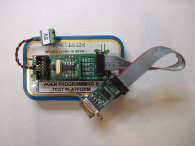
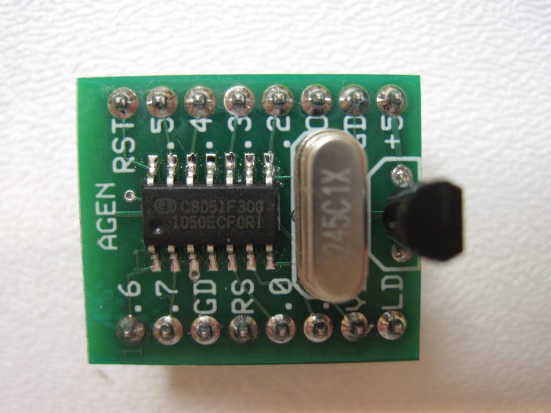
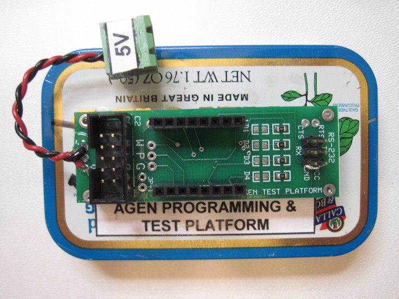
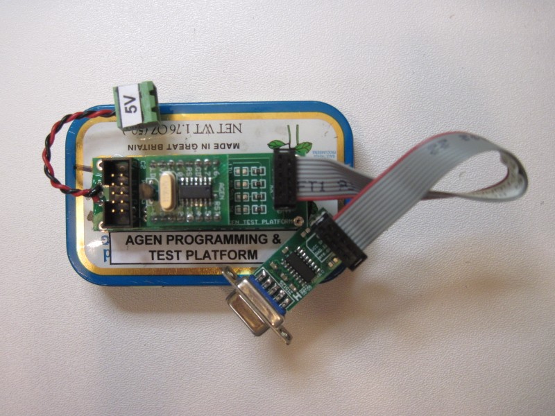
Photo 1 shows a completed ATAR Module (board is labeled "AGEN"), populated with a 300 chip and crystal. Photo 2 shows an ADEV Test/Programming Module mounted on a weighted breath mint tin and with a 5-Volt power umbilical. Photo 3 shows a complete development system, including a Target Module and a commercial RS-232 adaptor.
Page 3
For the following, refer to Schematic 1 titled "ATAR TARGET MODULE & TEST/PROGRAMMING BOARD." The schematic shows the components, circuitry and pinouts for the ATAR module and the wiring of the Test/Programming Board. Also shown is the wiring and board layout for the "pinking" network used for the AGEN Module. In other applications, the pads for this network can be used for general-purpose wiring of an RC network or left unpopulated.
You can also download Schematic 1 as a zip file.
The Parts List provides additional information about the components used to assemble the board.
The ATAR module measures approximately 3/4 by 7/8 inches (19 by 23 mm). As shown in the schematic, signal connections are available at two single row pin headers located on the board's long edge.
All processor port pins are available at the two 8-pin edge connectors, as are power input (e.g., 5 Volts), power out (3.3 Volts) and reset.
A footprint for an optional external HC49/US crystal and its support components are provided below the chip. The crystal oscillator pins (P0.2 and P0.3) are brought out to edge pins. One of these pins can be used for an external oscillator input (e.g., with a 600 chip) or both pins can be configured for general purpose I/O if the crystal or other oscillator options are not used.
The ADEV board provides LEDs and limit resistors that can be used to test ATAR I/O pins that are configured for push-pull operation. The ATAR board pin labeled "LD" may be left open or wired to power or ground. When left open, the test LEDs do not load the I/O pins to which they are attached.
Wiring the "LD" pin to either a supply voltage or ground allows the port pins to be tested in either "sourcing" or "sinking" modes (wire to ground to source, wire to power positive voltage to sink). Note that the schematic shows the test LEDs in the "sinking" configuration (i.e., "LD" is connected to +3.3 Volts). To change to a "sourcing" configuration, reverse the diode polarities and connect "LD" to ground.
Although all of the capabilities of the 300 and 600 microprocessors are beyond the scope of this documentation, one important feature of both chips is that the port pins can sink up to a maximum of 100 milliamperes when configured as push-pull outputs (also reference the Power section).
Page 4
As previously mentioned, ATAR was designed for use with SL chips that use a 14-pin SOIC package and also have compatible pin connections. These chips include the 300 and 600 chips and their variants.
The board was originally designed to provide a platform for the AGEN audio generator that provides white and pink noise and an number of other fixed, crystal-controlled frequencies. However, the ATAR Target Module also provides a general purpose platform for the two target chips that can be powered up and used without having to wire the basic operational components such as a regulator and crystal oscillator. The board's DIP format, with two 0.1 inch header rows, is well suited to connections on a solderless breadboard or socketed wiring on a perforated board.
In addition to providing a convenient hardware development platform for the 300 and 600 chips, several programming files are furnished on the documentation disk to allow fast checkout of a completed ATAR 300 module. These files are Intel hex format files that can be downloaded to the ATAR Module when it is installed in the ADEV Module.
This provides an easy way to verify the functionality of port pins and commonly-used chip features such as the serial port and external crystal oscillator. The programming file for chips using the internal 24.5 MHz oscillator can also be used to test a 600 chip, but this is somewhat pointless because the chip cannot be re-programmed for the target application. However, the Test/Programming board can be used to exercise port and serial I/O on a 600 chip that has been programmed with a separate programmer.
To set up the completed module for operation, it is necessary only to supply it with power. Once supplied with 5 Volt power between the "+5" pin and the "GD" (ground) pin, the module can be used with your application.
The following sections describe power connections, chip programming and software test procedures.
Page 5
A completed ATAR Module populated with a 300 chip can be set up for programming by plugging it into the ADEV Test/Programming platform and connecting the Silicon Laboratories USB Debug Adaptor to the 10-pin shrouded connector on the Test/Programming board. The Test/Programming board must be also be connected to 5 Volt power at the "POWER INPUT" connection pads.
These pads have duplicate ground pins so that a connector using 0.2 inch spacing can be installed directly on the board. Alternatively, stake pins or a polarized Molex header can be installed at the power connector pins. The outer ground pin can also be cut off and used to polarize a symmetrical 3-pin socket that has a plug installed on the outermost socket pin.
before programming the ATAR module, select one of the two test programs to download. These options are: External Crystal Oscillator or Internal Oscillator. With both of these options, the chip can be exercised with a terminal program and a serial port operating at a rate of 9600 baud (8 data bits, no parity, one stop bit -- 8N1)
The programming files for these board programming options on the documentation disk in the adev/software directory.
External Crystal Oscillator -- To test the Target chip (ATAR module) with a 24.576 MHz external crystal oscillator, use adev_X.hex file on the documentation disk.
Internal Oscillator -- To verify the Target chip (ATAR module) with the chip's internal oscillator, load the adev_25X.hex file on the documentation disk.
Web users can download adev_hex.zip to get the internal and external oscillator programming files.
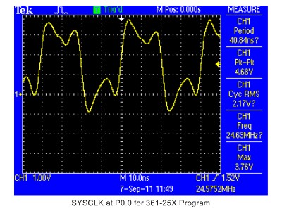
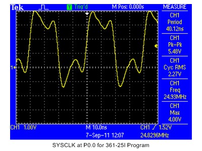
To program the module using the USB Debug Adaptor, bring up the Silicon Labs IDE and select the Connections/Connection Options menu item. This will bring up the connection options dialog. Select the "c2" and "USB Debug Adapter" radio buttons and exit the dialog. This is a one-time configuration and need not be changed each time you bring up the IDE. Next, select the Debug/Connect menu item. The module should connect to the IDE, as indicated by a "Target: C8051F300" indication at the bottom of the IDE's screen. Once connected, the chip can be programmed by selecting the Debug/Download Object File option. This will bring up a dialog that allows you to erase the chip (always do this) and download an object file from a selected directory (i.e., wherever the programming files are located). Once the module has been programmed, select the Debug/Disconnect menu option to disconnect the programmer from the USB Debug Adaptor. To test the programmed chip, connect the serial interface to a terminal program operating a 9600 baud. This will allow you to issue commands that exercise selected port outputs. See the Interactive Test section for details on the use of the serial port to interactively test the module in either the internal or external oscillator configurations. To use the interactive program options given above, an RS-232 level converter must be attached to port pins P0.4 (transmit output from the chip) and P0.5 (receive input from the PC). A number of inexpensive adaptors that perform this function are available on EBay. The Test/Programming Board has a connection footprint that allows direct connection of one of the most popular adaptors (e.g., by soldering the board's stake pins directly to the Test/Programming board). The RS-232 converter can also be attached to the Test/Programming board with a short 10-conductor ribbon cable, as shown in Photo 3. Note that the connection is performed with just the first six pins of the cable connectors (the remaining pins are not used). Ensure that pin 1 of each connector (usually marked with a triangle) connects to the pin marked "VCC" on the adaptor and on the Test/Programming Board. Caution: not all 10-pin cables are assembled in the same way -- we recommend that connections be verified with a continuity tester before initial power-up and use. Connection of the adaptor to the board can vary and comprehensive connection procedures are beyond the scope of this document. Serial Output -- The operation of the serial output of the chip can be verified without an adaptor by connecting an oscilloscope to the port pin labeled ".4" on the ATAR Module (P0.4). If the ATAR Module is installed on the Test/Programmer board, you can observe serial output on the pin marked "RX" on the Test/Programmer Board's RS-232 connection pads. Note that the "TX" and "RX" labels on the Test/Programming board are "PC centric" which is reversed from the normal convention for our schematics. This was done to avoid a conflict between the silk screening on the Test/Programming board and the silk screening on the RS-232 adaptor board. Thus, "RX" is the transmit output from the processor on the ATAR board and is also the receive input to the PC. At startup, when power is first applied to the module, an ATAR Module loaded with one of the test programs (such as adev_25X.hex) will output a string of characters giving the version and configuration. Thus, serial activity on port pin P0.4 at startup will provide a basic indication that the chip has an operable serial port. SYSCLK -- For both program options, the chip's SYSCLK output is routed to port pin P0.0. Observing this pin with an oscilloscope, or measuring it with a frequency counter, verifies that the chip is running. For the 25 MHz crystal option, the SYSCLK output should be at the crystal frequency, as shown by Photo 4 for a 24.576 MHz crystal output on P0.0. If the SYSCLK does not appear, ensure that the output is present without the crystal oscillator circuitry. This can be done by loading the adev_25I.hex programming file. This program option should work even if the crystal oscillator circuitry is inoperable (e.g., a bad crystal or incorrect capacitor values at C3 and C4). Photo 5 shows a typical SYSCLK output at P0.0 when the chip is operating with an internal clock. Note that Photo 4 and Photo 5 are for SYSCLK outputs from the C8051F361 chip on a MUTS Module but the outputs from an ATAR Module should be similar. The LEDs and limit resistors on the Test/Program Board may interfere with serial port testing because the LEDs are attached to P0[2,3] used by the crystal oscillator. To avoid this problem, ensure that the "LD" pin is open and not connected to power or ground. For interactive testing, P0.1 is configured as an error indicator and will rapidly flash an LED connected to it to indicate an error. If LEDs are connected to I/O ports, there may be conflicts with other I/O assigned to these pins. You may resolve these conflicts either by observing pins on a scope with no LED connection to the I/O pin, testing the module with the internal oscillator option or testing the module in a separate test environment (e.g., installed on your application board). The Test/Programming Board provides some testing flexibility but its configuration with indicator LEDs may not be compatible with all interactive test procedures. Serial Connection -- If the SYSCLK output is correct and the serial port appears to be operable, the chip can be verified interactively by connecting it through an RS-232 adaptor to a serial terminal program such as PuTTY. For both of the "25 MHz" options, the connection rate is 9600 baud (8,N,1). Error Indication -- When testing interactively, you may want to connect an LED (through a limiting resistor) to port P0.1. This port pin has been selected arbitrarily to act as an error indicator. When an LED is connected to the P0.1, the LED will rapidly flash when a non-fatal command error is encountered. Note that the Test/Programmer Board has an LED and limit resistor already connected to P0.1 for this purpose. In the following, commands will execute when the space bar is pressed or when the "Enter" key is pressed; pressing other keys will most likely produce an error and result in a program reset. Also note that successful commands are indicated by an "ok" response from the chip. Errors will either flash the error LED or reset the processor, depending on the type of the error and its severity. Design -- Before plunging into a description of the interactive commands, it may be useful to understand the design philosophy behind the interactive test programs. The programs are built around a command interpreter that is used for a number of BOBZ projects. The interpreter itself is rather simple, compiling to less than 600 bytes. But, this interpreter, along with a stack for temporary number storage, is sufficient to build an interactive command facility that can exercise chip ports and the serial port. Commands -- The number of commands is deliberately limited so that the program could function as a useful tool, not another command language to learn. In the interest of simplicity, commands were also defined single-characters (although multi-character equivalents can be entered). Once you learn how to put a hexadecimal number on the stack with the "$" command, you can exercise port I/O with the "t" command and serial I/O with the "e" command. Several other commands are included as a convenience but are not strictly necessary (e.g., the "d", "f" and "r" commands). It may take a minute or so to get used to executing commands with the space bar instead of the Enter key, but we think you will find it a very convenient entry method for single character commands. Of course, you can also enter commands in the "normal" fashion by using the Enter key. Once connected to a terminal at the correct baud rate, the version, configuration and help strings are output when power is applied to the module. The serial port input and output can be verified by entering a "h" at the keyboard (e.g., type an "h" and press the space bar). The "h" option displays the same information that is displayed when power is applied. To force a reset without cycling power, use the "r" command. Use the "f" command to flash the LED connected to P0.1 -- this flash is also used to indicate minor command errors. Note that P0.1 can also be toggled using the "t" and "x" commands, as described below. The easiest way to toggle a port pin is to use the "x" command. This command toggles all port pins that are valid for the current configuration. For example, using the "x" command while configured for the internal oscillator would toggle pins 1, 2, 3, 6 and 7; pins 0, 4, and 5 will not change because they are assigned to SYSCLK and the serial port. You can display all command options by entering the "help" or "h" commands. The Interactive Commands table provides a summary of other commands that can be entered interactively. You can put a byte on the command interpreter's stack. The stack is a "first in first out" local storage area that can be used to temporarily store data to be used with commands that require a parameter (e.g., the "e" and "t" commands). Parameter and data bytes are entered with the "$" command as hexadecimal digits. When the "$" command executes (i.e., when the space key is pressed) you can immediately enter two hexadecimal digits. The digits are echoed as they are entered. You can backspace during entry, but any entry error will result in a reset: when the interpreter resets, the stack is cleared and the help screen is displayed. Thus, to enter a byte to be put on the stack, enter "$", followed by a space and two hexadecimal digits (the digit range is 1-9 and a-f). After a value is put on the stack, its correct entry is confirmed with an "ok" response from the interpreter. You can use the "s" command to display the contents of the stack -- the number of items should increase by one as each byte is entered; the last byte entered will be the one shown nearest the ">" indicator. Once a hexadecimal number is on the stack, it can be used to toggle individual port pins with the "t" (toggle) command. To enter the port pin to be toggled, the number of the port is put on the stack, encoded as two hexadecimal digits. The first digit is the port number, the second digit is the pin number. Thus, putting the hexadecimal value of "01" on the stack, followed by the execution of the "t" command, will toggle port 0, pin 1. An easy way to verify the toggling command is to enter a hexadecimal value of 01 to specify P0.1, the port pin attached to the error LED. Repeated entry of the "t" command will toggle the error LED. Note that port pins assigned to other functions, such as SYSCLK (P0.0), the crystal oscillator (P0.2 and P0.3) or the serial port (P0.4 and P0.5) cannot be toggled with the "t" command. Because an ATAR module only has one port, and some pins are already assigned to other I/O, the only valid entries are 01, 02, 03, 06, and 07.
Putting the hexadecimal value of "07" on the stack followed by the execution of the "t" command will toggle port 0, pin 7 (P0.7). An easy way to verify the toggling command is to enter a hexadecimal value of 01 to specify P0.1, the port pin attached to the error LED. With a "1" on the stack, repeated entry of the "t" command will toggle the error LED. Note that port pins assigned to other functions, such as SYSCLK (P0.0), the crystal oscillator (P0.2 and P0.3 for the crystal option) or the serial port (P0.4 and P0.5) cannot be toggled with the "t" command. Thus, for the ATAR Module, only ports P0.1, P0.6 and P0.7 can be toggled with the atar_25X option. For the atar_25I option, P0.2 and P0.3 can also be toggled. Data bytes on the stack can also be used to exercise the serial port with the "e" (emit) command. For example, entering "$ 52" will put the hexadecimal value for the ASCII character "R" on the stack. Executing either the "e" or "emit" commands will display an "R" on the serial terminal's screen. If you have forgotton what values you have put on the stack, you can display the stack contents with the "s" command. This command displays the number of items on the stack (in hexadecimal), followed by a ">" character, followed by the values on the stack (in hexadecimal). For example, entering "$ 52 $ 77 $ 66 s" will result in a display that looks like this: 03> 66 77 52 . Note that the last item entered, the top of stack, is closest to the ">" indicator. If you want to put several duplicate items on the stack, use the "d" or "dup" (duplicate) commands. Thus, entering "$ 52" followed by a "dup" command puts two "R" characters on the stack. This can be seen by entering the "s" command after duplicating to get a stack display of: 02> 52 52 . To clear items from the stack, use the "r" command to reset the processor. Page 6Programming
Startup Testing
Interactive Test
Interactive Commands
| Duplicate the number on the top of the stack | |
| Send (emit) the top of stack character to the serial port | |
| Force an error condition (e.g., flash error LED on P1.1) | |
| Display version, configuration & commands | |
| Force a reset of the command interpreter | |
| Display number of stack items and their values in hexadecimal | |
| Toggle the port pin specified by the hex number on the top of the stack | |
| Example: with $11 on the stack, each time t is entered P1.1 will toggle | |
| Toggle all unassigned port bits | |
| Enter a hexadecimal number and put it on the top of the stack | |
| Notes: | |
| 1. Commands execute when the space bar or the "Enter" key are pressed | |
| 2. There are hidden commands (most of these execute without error) | |
| 3. Unsolicited version/configuration display indicates a reset | |
| 4. Port pins used for SYSCLK, crystal and serial port will not toggle | |
| 5. An LED wired to P1.1 acts as a visual error indicator |
Page 7
![]()
An on-board 3.3 Volt regulator provides stable regulated power to the Module. It operates with power inputs from 5 to 16 Volts. To configure the module for operation, connect either or both of the "GD" (ground) pins to the return of the supply (ground) and connect the "+5" pin to the input voltage (e.g., 5 Volts).
The module operates with power inputs from 5 to 16 Volts.
Although voltages higher than 5 Volts can be applied to the "+5" pin, the label was selected for compatibility with the Test/Programmer Board which operates at a supply voltage of 5 Volts.
Once the input voltage is applied between the "+5" and "GD" pins, the operation of the regulator can be verified by measuring the voltage between the GD (ground) and the "VDD" pin. The regulator output voltage should be close to 3.3 Volts. If you plan to operate the ATAR Module directly from an off-board supply, remove the regulator chip and install a jumper between the input and output pads. This, for example, could be used for an ATAR Module operating on a 3 Volt battery.
Module quiescent current draw will vary and is approximately 10 milliamperes at 24.5 MHz. Operating with a 32 kHz crystal, the module current can be as low as 65 microamperes. The maximum regulator output is 100 milliamperes.
Although the maximum current for the chip outputs is 500 milliamperes (total), with all outputs heavily loaded this is not possible with the 78L33 regulator. If the application requires currents higher than the 100 mA maximum of the regulator, an external regulator or high-current voltage source (e.g., a battery) must be used. To use an external regulator, remove the regulator chip and solder a wire across the regulator input and output pins before applying the externally-regulated power between the "+5" pin and either or both of the "GD" (ground) pins.
The chip digital outputs, when configured for push-pull operation, are rated for a maximum current of 100 milliamperes each with a maximum total chip current (including quiescent current draw) of 500 milliamperes. Chip outputs are 5 Volt tolerant.
Be aware that the total regulator dissipation is 250 milliwatts and the maximum regulator output is 100 milliamperes. We recommend that the dissipation be kept below half the dissipation limit and below the maximum current limit. The regulator is both current and temperature limited in the event of output overload.
Page 8
For board assembly procedures and hints, refer to the Assembly Guide.
We presently market ATAR only as an assembled and tested module. Thus, the hardware should work and most operational verification can be performed with the supplied software. If the module is configured with a crystal, normally the case, it is verified with the "25X" configuration. The chips are normally shipped with software loaded for either the internal or crystal configurations, depending on whether or not the crystal option is installed.
The internal oscillator for both the 300 and 600 chips is specified to be within 2% of 24.5 MHz. Thus, the serial port should work with the internal oscillator in the "25I" configuration.
We recommend testing a newly-finished board with the 300_25I.hex program before verifying the chip with a crystal oscillator program, 360_25X.hex. Probing pins P0[2,3] with an oscilloscope usually shows whether or not the crystal is operating but oscilloscope probe capacitance may interfere with oscillation. A better way to verify oscillator operation is to probe P0.0, which echos the system clock -- a 24.576 MHz square wave should appear at this pin if the 24.576 MHz crystal is oscillating properly.
If the chip does not operate in the crystal mode, verify the crystal's specification for maximum shunt capacitance. The schematic shows two 22 pF capacitors across the crystal but this applies only to the 24.575 MHz crystals we use for assembled units or crystals furnished with semi-kits. We have found that crystals may not oscillate if this capacitance is significantly more or less than the capacitance specified by the manufacturer.
There is a jumper position labeled "JP1" near the programming interface connector, P3. This jumper can be used to connect pin 10 of the programming connector and the "+5" power input. This jumper, when connected, furnishes 3.3 Volt power from the Debug adapter. This jumper is not normally installed. When used, do not connect power to the "POWER INPUT" and note that the serial adaptor may not operate properly (most adaptors operate from +5 Volts).
Page 9
The following parts list is for the ATAR Module populated with the "pinking" network for use with the AUDIT Audio Test Module.
| Part | |||||
| R1 | RES, 10M, 1/8W, 1%, 0805 | Mouser | 140-CC501N180J-RC |
||
| R2 | RES, 300R, 1/8W, 1%, 0805 | Digikey | 541-300CCT-ND |
||
| R3, R6, R7 & R13 | RES, 1K, 1/8W, 1%, 0805 | Digikey | 541-1.00KCCT-ND |
||
| R4 | RES, 3K, 1/8W, 1%, 0805 | Digikey | 541-3.00KCCT-ND |
||
| R5 | RES 6.8K, 1/8W, 1%, 0805 | Digikey | 541-6.8KCCT-ND |
||
| R9, R10, R11 & R12 | RES 120 Ohm, 1/8W, 1%, 0805 | Digikey | 541-120CCT-ND |
||
| C1 | CAP, 10uF, 10V, X5R, 0805 | Digikey | 490-1709-1-ND |
||
| C2, C9 | CAP, ceramic, 1uF, 25V, Y5V, 0805 | Digikey | C2012Y5V1E105Z/0.85 |
||
| C3, C4 | CAP, 22 pF, 50V, 5%, COG/NPO, 0805 | Mouser | 140-CC501N220J-RC |
||
| C5 | CAP, 0.033uF/50V, 10%, 0805 | Digikey | 490-1660-1-ND |
||
| C6, C7 | CAP, 0.047uF/25V, 10%, 0805 | Mouser | 81-GRM40X473K25D |
||
| C8 | CAP, 0.27uF/16V, 10%, 0805 | Mouser | 77-VJ0805Y274KXJRBC |
||
| C10 | CAP, 0.1uF/25V, 10%, 1206 | Stock | N/A |
||
| U1 | REG, 3.3 Volt, TO-92, 100 mA, 250 mW | Digikey | 497-7288-ND |
||
| U2 | IC, C8051F300GS microprocessor, pre-programmed | Digikey | 336-1535-5-ND |
||
| PCB | PCB, AGEN | ||||
| P1, P2 | HDR, 17-pin header, SIL, breakaway | FRYS | PLS-40S-P5 |
||
| P3 | HDR, 10-pin (2x5) shrouded header | stock | N/A |
||
| XTAL | XTAL, 24.576 MHz crystal, +/- 20 ppm, HC49/US | Mouser | 815-ABL-24.576-B2F |
Page 10
Original circuit, Rev. B of the schematic |